Introduction to PCB Copper Boards
Printed Circuit Boards (PCBs) are the backbone of modern electronic devices, providing a platform for components to be mounted and interconnected. One of the most crucial elements of a PCB is the copper board, which serves as the conductive layer for electrical signals to travel between components. In this comprehensive article, we will delve into the world of PCB copper boards, exploring their properties, manufacturing processes, and applications.
What is a PCB Copper Board?
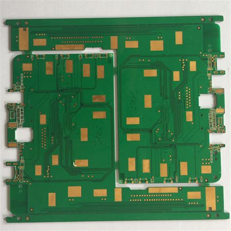
A PCB copper board is a thin layer of copper laminated onto an insulating substrate, typically made of fiberglass or epoxy resin. The copper layer is etched to create conductive tracks, pads, and other features that allow electronic components to be soldered and connected. The insulating substrate provides mechanical support and electrical isolation between the copper traces.
Properties of PCB Copper Boards
PCB copper boards exhibit several essential properties that make them suitable for use in electronic circuits:
- Electrical Conductivity: Copper is an excellent electrical conductor, allowing signals to travel with minimal resistance and loss.
- Thermal Conductivity: Copper’s high thermal conductivity helps dissipate heat generated by electronic components, preventing overheating and ensuring reliable operation.
- Mechanical Strength: When laminated onto a substrate, copper provides additional mechanical strength to the PCB, enabling it to withstand the stresses of manufacturing and use.
- Corrosion Resistance: Copper is naturally resistant to corrosion, ensuring the longevity and reliability of the PCB.
Manufacturing Process of PCB Copper Boards
The manufacturing process of PCB copper boards involves several steps, each critical to ensuring the quality and functionality of the final product.
Substrate Preparation
The first step in manufacturing a PCB copper board is to prepare the insulating substrate. The substrate, typically made of fiberglass or epoxy resin, is cut to the desired size and shape. Holes are drilled into the substrate to accommodate through-hole components and provide interconnections between layers in multi-layer boards.
Copper Lamination
Once the substrate is prepared, a thin layer of copper foil is laminated onto one or both sides of the substrate using heat and pressure. The copper foil is typically pre-coated with an adhesive to ensure a strong bond with the substrate. The thickness of the copper layer can vary depending on the application, with common thicknesses ranging from 0.5 oz to 2 oz per square foot.
Photoresist Application
To create the desired copper patterns on the PCB, a photoresist layer is applied to the copper surface. The photoresist is a light-sensitive material that hardens when exposed to ultraviolet (UV) light. The photoresist can be applied using various methods, such as screen printing, spin coating, or dry film lamination.
Exposure and Development
Once the photoresist is applied, the PCB is exposed to UV light through a photomask, which contains the desired copper pattern. The areas of the photoresist exposed to UV light harden, while the unexposed areas remain soluble. The PCB is then developed in a chemical solution, removing the soluble photoresist and revealing the copper pattern.
Etching
With the copper pattern exposed, the PCB undergoes an etching process to remove the unwanted copper. The most common etching method is chemical etching, where the PCB is immersed in an etchant solution, typically ferric chloride or ammonium persulfate. The etchant dissolves the exposed copper, leaving only the desired copper traces and features.
Photoresist Removal and Surface Finish
After etching, the remaining photoresist is removed using a chemical stripper, revealing the final copper pattern. To protect the copper from oxidation and improve solderability, a surface finish is applied. Common surface finishes include:
- Hot Air Solder Leveling (HASL): A thin layer of solder is applied to the copper surface and leveled using hot air.
- Electroless Nickel Immersion Gold (ENIG): A layer of nickel is deposited onto the copper, followed by a thin layer of gold.
- Organic Solderability Preservative (OSP): A thin, organic coating is applied to the copper to prevent oxidation.
Types of PCB Copper Boards
PCB copper boards can be categorized based on the number of copper layers and the arrangement of components.
Single-Layer PCBs
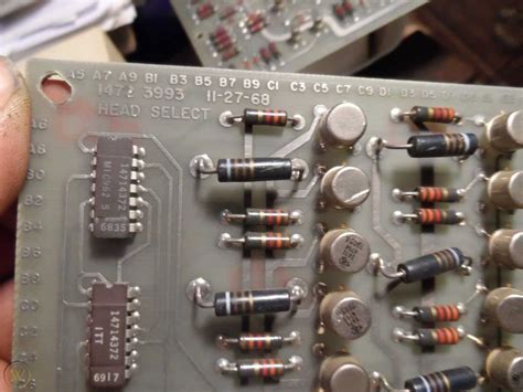
Single-layer PCBs have copper on only one side of the substrate. They are the simplest and most cost-effective type of PCB, suitable for low-complexity circuits with a limited number of components. Single-layer PCBs are commonly used in consumer electronics, such as remote controls and simple toys.
Double-Layer PCBs
Double-layer PCBs have copper on both sides of the substrate, allowing for more complex circuits and higher component density. The two copper layers are interconnected using through-holes, which are plated with copper to provide electrical continuity. Double-layer PCBs are widely used in a variety of applications, from industrial control systems to consumer electronics.
Multi-Layer PCBs
Multi-layer PCBs consist of three or more copper layers laminated together with insulating layers in between. These boards offer the highest component density and signal routing complexity, making them ideal for advanced electronic devices such as smartphones, computers, and medical equipment. Multi-layer PCBs can have up to 50 layers or more, depending on the application requirements.
Flexible PCBs
Flexible PCBs, also known as flex circuits, use a flexible substrate material, such as polyimide or polyester, instead of the rigid fiberglass or epoxy resin. The copper layers are laminated onto the flexible substrate, allowing the PCB to bend and conform to the shape of the device. Flexible PCBs are commonly used in applications that require compact packaging or movable parts, such as camera modules, wearable devices, and automotive electronics.

Applications of PCB Copper Boards
PCB copper boards are used in virtually every electronic device, from simple consumer gadgets to complex industrial systems. Some of the most common applications include:
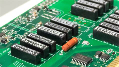
- Consumer Electronics: Smartphones, laptops, televisions, home appliances, and gaming consoles all rely on PCB copper boards for their functionality.
- Automotive Electronics: Modern vehicles incorporate numerous electronic systems, such as engine control units, infotainment systems, and advanced driver assistance systems (ADAS), all of which use PCB copper boards.
- Medical Devices: PCB copper boards are essential components in medical equipment, including patient monitors, diagnostic tools, and implantable devices.
- Industrial Control Systems: Automation and process control systems in factories, power plants, and other industrial settings rely on PCB copper boards for reliable operation.
- Aerospace and Defense: PCB copper boards are used in various aerospace and defense applications, such as avionics, satellite systems, and military communications equipment.
Advancements in PCB Copper Board Technology
As electronic devices continue to evolve, so do PCB copper board technologies. Some of the latest advancements in the field include:
High-Density Interconnect (HDI) PCBs
HDI PCBs feature finer trace widths and smaller via sizes, enabling higher component density and improved signal integrity. These boards are essential for creating compact, high-performance electronic devices, such as smartphones and wearables.
Embedded Components
Embedded component technology allows passive components, such as resistors and capacitors, to be embedded within the PCB substrate. This approach saves space on the board surface, reduces signal path length, and improves overall device performance.
3D Printed Electronics
3D printing technology is being explored for the fabrication of PCB copper boards, offering the potential for rapid prototyping, customization, and complex geometries. Conductive inks and filaments containing copper particles are used to create the conductive traces and features on the PCB.
Advanced Materials
Researchers are continuously developing new materials for PCB substrates and copper traces to improve performance and reliability. Some examples include:
- Low-loss dielectrics for high-frequency applications
- Thermally conductive substrates for better heat dissipation
- Copper alloys with enhanced mechanical and electrical properties
PCB Copper Board Design Considerations
When designing a PCB copper board, several factors must be considered to ensure optimal performance and manufacturability.
Trace Width and Spacing
The width of the copper traces and the spacing between them are critical parameters in PCB design. Trace width determines the current-carrying capacity and resistance of the trace, while spacing affects signal integrity and the potential for crosstalk between adjacent traces. Designers must follow industry standards and guidelines, such as the IPC-2221 standard, to ensure proper trace width and spacing for a given application.
Via Design
Vias are plated holes that provide electrical connections between layers in a multi-layer PCB. Via design considerations include the size, placement, and type of via (through-hole, blind, or buried). Proper via design ensures reliable inter-layer connections and minimizes signal integrity issues, such as reflections and crosstalk.
Impedance Control
For high-speed digital circuits and radio frequency (RF) applications, controlling the impedance of the copper traces is essential to maintain signal integrity and minimize reflections. Impedance is determined by factors such as trace width, thickness, and the dielectric constant of the substrate material. Designers use specialized software tools to calculate and optimize trace dimensions for a target impedance.
Thermal Management
Effective thermal management is crucial for ensuring the reliability and longevity of electronic components. PCB copper boards play a significant role in heat dissipation, as the copper traces and planes can act as thermal pathways. Designers must consider factors such as copper thickness, trace layout, and the use of thermal vias to optimize heat transfer from components to the environment.
Signal Integrity and EMI/EMC
Maintaining signal integrity and minimizing electromagnetic interference (EMI) and electromagnetic compatibility (EMC) issues are critical aspects of PCB copper board design. Designers must consider factors such as trace routing, ground plane design, and the use of shielding and filtering components to mitigate EMI/EMC problems and ensure reliable signal transmission.
Quality Control and Testing of PCB Copper Boards
To ensure the reliability and functionality of PCB copper boards, rigorous quality control and testing procedures are employed throughout the manufacturing process.
Visual Inspection
Visual inspection is the first line of defense in detecting manufacturing defects. Automated optical inspection (AOI) systems use high-resolution cameras and image processing algorithms to identify issues such as missing components, incorrect component placement, and solder defects.
Electrical Testing
Electrical testing verifies the continuity and isolation of the copper traces and ensures that the PCB functions as intended. Common electrical tests include:
- Continuity Test: Verifies that all intended connections are present and have low resistance.
- Isolation Test: Ensures that there are no unintended short circuits between copper traces or layers.
- Functional Test: Checks the PCB’s performance under real-world operating conditions, often using a bed-of-nails fixture or flying probe tester.
Environmental Testing
Environmental testing subjects the PCB to various stresses to ensure its reliability and durability. Common environmental tests include:
- Thermal Cycling: Exposes the PCB to alternating high and low temperatures to simulate thermal stress during operation.
- Humidity Testing: Verifies the PCB’s resistance to moisture and humidity-related issues, such as corrosion and delamination.
- Vibration and Shock Testing: Assesses the PCB’s ability to withstand mechanical stresses encountered during transport and use.
Automated Optical Inspection (AOI)
AOI systems use high-resolution cameras and advanced image processing algorithms to detect manufacturing defects, such as solder bridges, missing components, and incorrect component placement. AOI is a fast and reliable method for identifying issues early in the manufacturing process, reducing the need for manual inspection and increasing overall quality.
X-Ray Inspection
X-ray inspection is used to detect defects that are not visible on the surface of the PCB, such as voids in solder joints, misaligned ball grid array (BGA) packages, and internal delamination. X-ray systems provide a non-destructive means of evaluating the quality of hidden features, ensuring the reliability of the PCB.
Frequently Asked Questions (FAQ)
-
What is the difference between a single-layer and a double-layer PCB copper board?
A single-layer PCB has copper on only one side of the substrate, while a double-layer PCB has copper on both sides. Double-layer PCBs offer more design flexibility and higher component density compared to single-layer boards. -
What is the purpose of solder mask on a PCB copper board?
Solder mask is a protective coating applied to the copper surface of a PCB, leaving only the exposed pads and holes for soldering. It helps prevent solder bridges, protects the copper from oxidation, and provides electrical insulation between traces. -
Can PCB copper boards be recycled?
Yes, PCB copper boards can be recycled. The recycling process typically involves shredding the boards and separating the metals, such as copper and gold, from the non-metallic components. The recovered metals can then be used in the production of new PCBs or other products. -
What is the typical thickness of the copper layer on a PCB?
The thickness of the copper layer on a PCB is typically measured in ounces per square foot (oz/ft²). Common thicknesses include 0.5 oz, 1 oz, and 2 oz copper, which correspond to approximately 17.5 μm, 35 μm, and 70 μm, respectively. -
How do I choose the right surface finish for my PCB copper board?
The choice of surface finish depends on factors such as the application requirements, soldering process, and environmental conditions. HASL is a cost-effective option for general-purpose applications, while ENIG provides excellent solderability and shelf life for high-reliability applications. OSP is a good choice for low-cost, lead-free assemblies.
Conclusion
PCB copper boards are the foundation of modern electronic devices, providing the conductive pathways for electrical signals to travel between components. Understanding the properties, manufacturing processes, and design considerations of PCB copper boards is essential for creating reliable, high-performance electronic products.
As technology continues to advance, PCB copper board manufacturing and design techniques are evolving to meet the ever-increasing demands for miniaturization, high-speed operation, and reliability. By staying up-to-date with the latest advancements and best practices in PCB copper board technology, designers and manufacturers can create innovative electronic solutions that drive progress across a wide range of industries.
No responses yet