Introduction to PCB Coplanar Waveguides
Coplanar waveguides (CPWs) are a type of transmission line widely used in high-frequency printed circuit board (PCB) designs. They consist of a central signal conductor strip flanked by two ground planes on the same surface of a dielectric substrate. CPWs offer several advantages over other transmission line structures, such as microstrip and stripline, including lower dispersion, better isolation, and easier integration with active components.
Advantages of Coplanar Waveguides
- Low dispersion: CPWs exhibit lower dispersion compared to microstrip lines, making them suitable for high-frequency applications where signal integrity is crucial.
- Improved isolation: The ground planes on either side of the signal conductor provide better isolation from adjacent signal traces, reducing crosstalk.
- Ease of integration: Active components can be easily mounted on CPWs without the need for via holes, simplifying the PCB layout and reducing parasitic effects.
Applications of Coplanar Waveguides
Coplanar waveguides find applications in various high-frequency and high-speed electronic systems, such as:
- Microwave and millimeter-wave circuits
- High-speed digital interconnects
- RF and wireless communication devices
- Optical and optoelectronic components
PCB Coplanar Waveguide Design Considerations
When designing coplanar waveguides on PCBs, several factors must be taken into account to ensure optimal performance and signal integrity.
Characteristic Impedance
The characteristic impedance of a coplanar waveguide is determined by the width of the signal conductor, the gap between the signal conductor and ground planes, and the dielectric constant of the substrate. The most common characteristic impedance values for CPWs are 50 Ω and 75 Ω, which match the impedance of standard RF and microwave components.
To calculate the characteristic impedance of a CPW, the following equation can be used:
$Z_0 = \frac{30\pi}{\sqrt{\varepsilon_{eff}}} \frac{K(k’)}{K(k)}$
where:
– $Z_0$ is the characteristic impedance
– $\varepsilon_{eff}$ is the effective dielectric constant
– $K(k)$ and $K(k’)$ are complete elliptic integrals of the first kind
– $k = \frac{a}{b}$ and $k’ = \sqrt{1 – k^2}$
– $a$ is the width of the signal conductor
– $b$ is the distance between the outer edges of the ground planes
Effective Dielectric Constant
The effective dielectric constant ($\varepsilon_{eff}$) of a coplanar waveguide depends on the substrate’s dielectric constant and the geometry of the conductors. It can be calculated using the following equation:
$\varepsilon_{eff} = 1 + \frac{\varepsilon_r – 1}{2} \frac{K(k’)}{K(k)} \frac{K(k_1)}{K(k_1′)}$
where:
– $\varepsilon_r$ is the dielectric constant of the substrate
– $k_1 = \sinh(\pi a / 2h) / \sinh(\pi b / 2h)$
– $k_1′ = \sqrt{1 – k_1^2}$
– $h$ is the thickness of the substrate
Conductor Width and Gap
The width of the signal conductor and the gap between the signal conductor and ground planes are critical parameters in CPW design. They determine the characteristic impedance and the cutoff frequency of the waveguide.
To achieve a desired characteristic impedance, the conductor width and gap can be adjusted using the following equations:
$a = b \frac{K(k)}{K(k’)}$
$g = b – a$
where:
– $a$ is the width of the signal conductor
– $b$ is the distance between the outer edges of the ground planes
– $g$ is the gap between the signal conductor and ground planes
It is essential to maintain a consistent conductor width and gap along the length of the CPW to avoid impedance discontinuities and reflections.
Substrate Selection
The choice of substrate material is crucial in CPW design, as it affects the waveguide’s electrical properties and performance. The substrate’s dielectric constant and loss tangent should be considered when selecting a material.
Common substrate materials for high-frequency PCBs include:
- Rogers RO4000 series: Low-loss, high-frequency laminates with stable dielectric constant
- Taconic RF-35: Low-loss, high-frequency laminate with low moisture absorption
- PTFE (Teflon): Low-loss, high-frequency material with excellent thermal stability
The substrate thickness should be chosen based on the desired characteristic impedance and the frequency range of operation. Thinner substrates are generally preferred for higher frequencies to minimize radiation losses and dispersion.
Grounding and Shielding
Proper grounding and shielding techniques are essential for optimal CPW performance. The ground planes should be connected to a low-impedance ground reference using multiple via holes along the length of the waveguide. This minimizes ground bounce and ensures a stable reference plane.
Shielding can be implemented using via fences or solid metal planes on adjacent layers of the PCB. This helps to reduce electromagnetic interference (EMI) and crosstalk between adjacent signal traces.
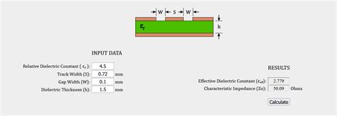
PCB Coplanar Waveguide Calculator
To simplify the design process, a PCB coplanar waveguide calculator can be used to determine the necessary conductor dimensions for a given characteristic impedance and substrate material.
Input Parameters
- Substrate dielectric constant ($\varepsilon_r$)
- Substrate thickness ($h$)
- Desired characteristic impedance ($Z_0$)
- Operating frequency ($f$)
Output Parameters
- Signal conductor width ($a$)
- Gap between signal conductor and ground planes ($g$)
- Effective dielectric constant ($\varepsilon_{eff}$)
- Cutoff frequency ($f_c$)
Calculator Algorithm
- Calculate the ratio $k$ based on the desired characteristic impedance and the substrate’s dielectric constant using numerical methods or lookup tables.
- Determine the distance between the outer edges of the ground planes ($b$) using the following equation:
$b = \frac{h}{\pi} \sinh^{-1}\left(\frac{1}{\sinh(\pi a / 2h)}\right)$
- Calculate the signal conductor width ($a$) and gap ($g$) using the equations provided in the “Conductor Width and Gap” section.
- Calculate the effective dielectric constant ($\varepsilon_{eff}$) using the equation provided in the “Effective Dielectric Constant” section.
- Determine the cutoff frequency ($f_c$) using the following equation:
$f_c = \frac{c}{4a\sqrt{\varepsilon_{eff}}}$
where $c$ is the speed of light in vacuum.
- Display the output parameters.
Calculator Usage
To use the PCB coplanar waveguide calculator:
- Enter the substrate’s dielectric constant, thickness, desired characteristic impedance, and operating frequency.
- Click the “Calculate” button.
- The calculator will display the signal conductor width, gap, effective dielectric constant, and cutoff frequency.
- Adjust the input parameters as needed to optimize the CPW design.

PCB Coplanar Waveguide Manufacturing Considerations
When manufacturing PCBs with coplanar waveguides, several factors should be considered to ensure the best possible performance.
Conductor Surface Finish
The surface finish of the conductors plays a crucial role in high-frequency performance. Smooth, low-profile finishes, such as immersion silver (IAg) or electroless nickel immersion gold (ENIG), are preferred to minimize skin effect losses and surface roughness.
Dielectric Laminate Selection
The choice of dielectric laminate should be based on the desired electrical properties and the manufacturing process. Low-loss, high-frequency laminates, such as Rogers RO4000 series or Taconic RF-35, offer excellent performance but may require specialized processing techniques.
Standard FR-4 laminates can be used for lower-frequency applications, but their higher dielectric loss and moisture absorption should be considered.
Controlled Impedance Manufacturing
To maintain the desired characteristic impedance along the length of the CPW, controlled impedance manufacturing techniques should be employed. This involves precise control of the conductor width, gap, and substrate thickness during the PCB fabrication process.
Specialized equipment, such as impedance-controlled etching systems and laser direct imaging (LDI), can be used to achieve tight tolerances on conductor dimensions.
Via Hole Placement and Size
Via holes are used to connect the ground planes of the CPW to the ground reference plane on other layers of the PCB. The placement and size of the via holes should be carefully considered to minimize discontinuities and reflections.
Via holes should be placed close to the edges of the ground planes and spaced regularly along the length of the waveguide. The diameter of the via holes should be kept small to reduce parasitic inductance and capacitance.
Conclusion
Coplanar waveguides are an essential component of high-frequency PCB design, offering advantages such as low dispersion, improved isolation, and ease of integration with active components. When designing CPWs, factors such as characteristic impedance, effective dielectric constant, conductor width and gap, substrate selection, and grounding and shielding should be carefully considered.
A PCB coplanar waveguide calculator can be a valuable tool for determining the necessary conductor dimensions based on the desired characteristic impedance and substrate properties. Proper manufacturing techniques, including conductor surface finish, dielectric laminate selection, controlled impedance manufacturing, and via hole placement and size, are crucial for achieving optimal CPW performance.
By understanding the principles of coplanar waveguide design and utilizing appropriate tools and manufacturing methods, PCB designers can create high-performance, high-frequency circuits for a wide range of applications.
Frequently Asked Questions (FAQ)
-
Q: What is a coplanar waveguide (CPW)?
A: A coplanar waveguide is a type of transmission line used in high-frequency PCB design, consisting of a central signal conductor strip flanked by two ground planes on the same surface of a dielectric substrate. -
Q: What are the advantages of using coplanar waveguides in PCB design?
A: Coplanar waveguides offer several advantages, including lower dispersion, better isolation from adjacent signal traces, and easier integration with active components compared to other transmission line structures like microstrip and stripline. -
Q: How does the characteristic impedance of a coplanar waveguide affect its performance?
A: The characteristic impedance of a coplanar waveguide determines how well it matches the impedance of connected components and how efficiently power is transferred. Mismatched impedances can lead to reflections, signal distortion, and power loss. -
Q: What factors should be considered when selecting a substrate material for coplanar waveguides?
A: When selecting a substrate material for coplanar waveguides, factors such as dielectric constant, loss tangent, thickness, and thermal stability should be considered. Low-loss, high-frequency materials like Rogers RO4000 series or Taconic RF-35 are often preferred for optimal performance. -
Q: How can a PCB coplanar waveguide calculator assist in the design process?
A: A PCB coplanar waveguide calculator can help determine the necessary conductor width and gap for a desired characteristic impedance and substrate material. By inputting parameters such as dielectric constant, substrate thickness, and operating frequency, the calculator provides output values that can be used to optimize the CPW design.
No responses yet