Introduction to PCB Circuit Boards
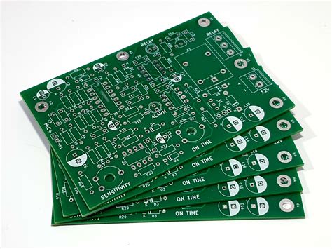
Printed Circuit Boards, commonly known as PCBs, are the backbone of modern electronics. These boards are used in almost every electronic device, from smartphones and computers to home appliances and industrial equipment. PCBs provide a way to mechanically support and electrically connect electronic components using conductive pathways, tracks, or signal traces etched from copper sheets laminated onto a non-conductive substrate.
In this beginner’s guide, we’ll walk you through the basics of PCB circuit boards, including their types, design process, and how to get started with creating your own PCBs.
Types of PCB Circuit Boards
There are several types of PCB circuit boards, each with its own unique characteristics and applications. Here are the most common types:
Single-Layer PCBs
Single-layer PCBs have conductive traces on only one side of the board. They are the simplest and most cost-effective type of PCB, making them ideal for basic electronic projects and low-density designs.
Double-Layer PCBs
Double-layer PCBs have conductive traces on both sides of the board, allowing for more complex designs and higher component density compared to single-layer PCBs. These boards are commonly used in consumer electronics and more advanced projects.
Multi-Layer PCBs
Multi-layer PCBs consist of three or more conductive layers, with insulating layers separating them. These boards are used for highly complex designs that require high component density and advanced signal routing, such as in smartphones, computers, and industrial equipment.
Flexible PCBs
Flexible PCBs are made from flexible materials, such as polyimide, allowing them to bend and conform to various shapes. They are often used in applications where space is limited or where the board needs to fit into a specific form factor, such as in wearable devices and medical equipment.
Rigid-Flex PCBs
Rigid-flex PCBs combine the benefits of both rigid and flexible PCBs. They consist of rigid sections connected by flexible sections, allowing for more complex designs and improved reliability in applications that require both stability and flexibility, such as in aerospace and military equipment.

PCB Design Process
The PCB design process involves several steps, from conceptualization to final production. Here’s an overview of the main stages:
Schematic Design
The first step in the PCB design process is to create a schematic diagram of the electronic circuit. This diagram represents the electrical connections between components and helps to ensure that the circuit will function as intended.
Component Selection
Once the schematic is complete, the next step is to select the appropriate components for the PCB. This involves choosing components that meet the required specifications, such as voltage rating, current rating, and package size.
PCB Layout
After selecting the components, the PCB layout process begins. This involves arranging the components on the board and routing the conductive traces between them. The layout process must take into account factors such as signal integrity, electromagnetic compatibility, and manufacturing constraints.
Design Rule Check (DRC)
Before finalizing the PCB layout, it’s essential to perform a Design Rule Check (DRC). This automated check ensures that the design meets the manufacturing constraints and design rules specified by the PCB fabricator, such as minimum trace width, minimum clearance between traces, and drill hole sizes.
Gerber File Generation
Once the PCB layout is finalized and has passed the DRC, the next step is to generate Gerber files. Gerber files are the industry-standard format for describing the PCB layout and are used by PCB fabricators to manufacture the board.
PCB Fabrication
The final step in the PCB design process is fabrication. The Gerber files are sent to a PCB fabricator, who uses them to manufacture the physical board. The fabrication process involves several stages, such as copper etching, drilling, plating, and solder mask application.

Getting Started with PCB Design Software
To design your own PCB circuit boards, you’ll need to use PCB design software. There are several options available, ranging from free and open-source software to professional-grade commercial tools. Here are some popular choices for beginners:
KiCad
KiCad is a free and open-source PCB design software suite that includes schematic capture, PCB layout, and Gerber file generation tools. It has a large community of users and extensive documentation, making it a great choice for beginners.
Eagle
Eagle is a popular PCB design software owned by Autodesk. It offers a free version for non-commercial use, as well as paid versions with advanced features. Eagle has a user-friendly interface and a large library of component footprints and symbols.
EasyEDA
EasyEDA is a web-based PCB design platform that offers schematic capture, PCB layout, and Gerber file generation tools. It has a free version with limited features and a paid version with advanced capabilities. EasyEDA also provides a built-in component library and a marketplace for ordering PCBs directly from manufacturers.

PCB Manufacturing and Assembly
After designing your PCB, the next step is to have it manufactured and assembled. There are several options for PCB manufacturing and assembly, depending on your needs and budget:
PCB Fabrication Houses
PCB fabrication houses specialize in manufacturing bare PCBs based on your Gerber files. They offer a range of options, such as different board materials, copper weights, and surface finishes. Some popular PCB fabrication houses include JLCPCB, PCBWay, and OSH Park.
PCB Assembly Services
PCB assembly services offer to manufacture and assemble your PCB, including sourcing components and soldering them onto the board. This can be a convenient option if you don’t have the equipment or expertise to assemble the PCB yourself. Some PCB fabrication houses, such as JLCPCB and PCBWay, also offer assembly services.
DIY PCB Assembly
If you have the necessary skills and equipment, you can assemble your PCB yourself. This involves sourcing components, soldering them onto the board, and testing the assembled PCB. DIY PCB assembly can be a cost-effective option for small-scale projects or prototypes.
Troubleshooting and Testing PCBs
After manufacturing and assembling your PCB, it’s essential to test and troubleshoot it to ensure that it functions as intended. Here are some common techniques for troubleshooting and testing PCBs:
Visual Inspection
The first step in troubleshooting a PCB is to perform a visual inspection. Look for any obvious defects, such as damaged components, solder bridges, or missing connections.
Multimeter Testing
A multimeter is a valuable tool for testing PCBs. It can be used to measure voltage, current, and resistance at various points on the board, helping to identify any issues with the circuit.
Oscilloscope Testing
An oscilloscope is used to visualize and analyze electrical signals on a PCB. It can be helpful for debugging issues related to signal integrity, such as noise, crosstalk, and reflections.
In-Circuit Testing
In-circuit testing involves using specialized equipment to test individual components on a PCB while they are still connected to the board. This technique can help identify faulty components or incorrect component values.
Functional Testing
Functional testing involves testing the PCB as a complete system to ensure that it performs its intended function. This may involve connecting the PCB to other components or devices and verifying that it operates correctly under various conditions.
Frequently Asked Questions (FAQ)
-
What is the difference between a PCB and a breadboard?
A breadboard is a prototyping tool used to build and test electronic circuits without soldering. It allows for quick and easy modification of the circuit. In contrast, a PCB is a more permanent solution, where the components are soldered onto a board designed specifically for that circuit. -
Can I design a PCB without using specialized software?
While it is possible to design a simple PCB by hand, using specialized PCB design software is highly recommended. These tools offer features such as schematic capture, component libraries, and design rule checking, which help to streamline the design process and reduce the risk of errors. -
What are the most common PCB manufacturing materials?
The most common PCB manufacturing material is FR-4, a glass-reinforced epoxy laminate. Other materials include aluminum for heat dissipation, flexible materials like polyimide for flexible PCBs, and high-frequency materials like Rogers for RF applications. -
How long does it typically take to manufacture a PCB?
The manufacturing time for a PCB depends on several factors, such as the complexity of the design, the chosen fabrication house, and the selected shipping method. Generally, PCB fabrication can take anywhere from a few days to a few weeks. -
What is the minimum feature size for a PCB?
The minimum feature size for a PCB depends on the capabilities of the PCB fabrication house. Most standard PCB fabricators can achieve a minimum trace width and spacing of around 6 mil (0.15 mm). However, advanced PCB fabricators can produce traces as narrow as 3 mil (0.08 mm) or even smaller for high-density designs.
Conclusion
PCB circuit boards are essential components in modern electronics, enabling the creation of complex and reliable electronic devices. By understanding the basics of PCB types, design processes, and manufacturing techniques, beginners can start exploring the world of PCB design and bring their electronic projects to life.
This guide has provided an overview of the key concepts and tools needed to get started with PCB design, as well as some practical tips for troubleshooting and testing PCBs. With the right knowledge and tools, anyone can learn to design and create their own PCB circuit boards.
No responses yet