What is PCB Assembly?
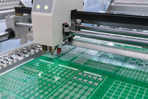
PCB assembly, also known as printed circuit board assembly or PCBA, is the process of attaching electronic components to a printed circuit board (PCB). This process involves several steps, including solder paste application, component placement, reflow soldering, and inspection. The goal of PCB assembly is to create a functional electronic device by connecting various components, such as resistors, capacitors, integrated circuits (ICs), and connectors, to the PCB.
Types of PCB Assembly
There are three main types of PCB assembly:
-
Through-Hole Assembly (THA): This is the traditional method of PCB assembly, where component leads are inserted through holes drilled in the PCB and soldered on the opposite side.
-
Surface mount assembly (SMT): In this method, components are placed directly onto the surface of the PCB and soldered using a reflow oven. SMT allows for smaller components and higher component density compared to THA.
-
Mixed assembly: This approach combines both through-hole and surface mount components on a single PCB, taking advantage of the benefits of both methods.
PCB Assembly Process
The PCB assembly process typically involves the following steps:
-
Solder paste application: Solder paste, a mixture of tiny solder particles and flux, is applied to the PCB’s pads using a stencil or solder paste printer.
-
Component placement: Components are placed onto the PCB using automated pick-and-place machines or manually, depending on the complexity and volume of the assembly.
-
Reflow soldering: The PCB with components is passed through a reflow oven, which melts the solder paste and creates a permanent connection between the components and the PCB.
-
Inspection: The assembLED PCB undergoes various inspections, such as visual inspection, automated optical inspection (AOI), and X-ray inspection, to ensure the quality and reliability of the assembly.
-
Testing: Functional testing is performed to verify that the assembled PCB operates as intended and meets the required specifications.
What is Defined Impedance?
Defined impedance, also known as controlled impedance, refers to the precise control of the characteristic impedance of a PCB’s signal traces. Characteristic impedance is the resistance to the flow of electrical signals through a transmission line, such as a PCB trace. Maintaining a consistent and specific characteristic impedance is crucial for high-speed digital circuits and radio frequency (RF) applications to ensure signal integrity and minimize signal reflections and distortions.
Factors Affecting Impedance
Several factors influence the characteristic impedance of a PCB trace:
-
Trace width: The width of the copper trace on the PCB.
-
Trace thickness: The thickness of the copper trace.
-
Dielectric constant: The property of the PCB substrate material that affects the speed of signal propagation.
-
Dielectric thickness: The distance between the signal trace and the reference plane (ground or power plane).
-
Trace spacing: The distance between adjacent traces on the same layer.
Calculating Characteristic Impedance
The characteristic impedance of a PCB trace can be calculated using various formulas, depending on the trace geometry and the PCB Stackup. The most common formulas are:
- Microstrip: For traces on the outer layers of the PCB, with a single reference plane:
$$Z_0 = \frac{87}{\sqrt{\varepsilon_r + 1.41}} \ln \left(\frac{5.98h}{0.8w + t}\right)$$
- Stripline: For traces embedded within the PCB, with two reference planes:
$$Z_0 = \frac{60}{\sqrt{\varepsilon_r}} \ln \left(\frac{1.9(2h)}{0.8w + t}\right)$$
Where:
– $Z_0$ is the characteristic impedance (in ohms)
– $\varepsilon_r$ is the dielectric constant of the PCB substrate
– $h$ is the dielectric thickness (in mils)
– $w$ is the trace width (in mils)
– $t$ is the trace thickness (in mils)
Common Impedance Values
The most common characteristic impedance values used in PCB design are:
| Impedance (Ω) | Application |
|---|---|
| 50 | RF circuits, high-speed digital interfaces |
| 75 | Video and cable television (CATV) applications |
| 90 | High-speed memory interfaces (DDR) |
| 100 | Ethernet, USB, and other high-speed interfaces |

PCB Stackup Design for Defined Impedance
To achieve defined impedance in a PCB design, the stackup must be carefully planned and optimized. A PCB stackup refers to the arrangement of copper layers, dielectric layers, and planes within the PCB. The stackup design affects the impedance, signal integrity, and manufacturability of the PCB.
Factors to Consider in Stackup Design
When designing a PCB stackup for defined impedance, consider the following factors:
-
Number of layers: The number of copper layers in the PCB, which depends on the complexity of the design and the required signal routing density.
-
Layer arrangement: The sequence of signal, ground, and power layers in the stackup, which affects the impedance and signal integrity.
-
Dielectric material: The choice of PCB substrate material, which determines the dielectric constant and affects the impedance and signal speed.
-
Dielectric thickness: The thickness of the dielectric layers between copper layers, which influences the impedance and the manufacturability of the PCB.
-
Copper weight: The thickness of the copper layers, typically expressed in ounces per square foot (oz/ft²), which affects the impedance and current-carrying capacity of the traces.
Example PCB Stackup for Defined Impedance
An example 6-layer PCB stackup optimized for defined impedance might look like this:
| Layer | Material | Thickness (mil) | Copper Weight (oz/ft²) |
|---|---|---|---|
| Top | Signal | 1.2 | 1 |
| 2 | Ground | 1.2 | 1 |
| 3 | Signal | 1.2 | 1 |
| 4 | Signal | 1.2 | 1 |
| 5 | Power | 1.2 | 1 |
| Bottom | Signal | 1.2 | 1 |
In this stackup, the signal layers are alternated with ground and power planes to provide a stable reference for impedance control. The dielectric thickness between layers is chosen to achieve the desired impedance, and the copper weight is selected to balance impedance and current-carrying requirements.

Designing PCBs with Defined Impedance
When designing PCBs with defined impedance, follow these best practices:
-
Determine the required impedance: Identify the target impedance value for each signal trace based on the application and the interface requirements.
-
Choose the appropriate PCB stackup: Select a stackup that provides the necessary number of layers, dielectric materials, and thicknesses to achieve the target impedance.
-
Calculate trace dimensions: Use impedance calculation formulas or PCB design software to determine the trace width and spacing required to achieve the target impedance.
-
Route signals carefully: Follow signal routing guidelines, such as minimizing trace length, avoiding sharp bends, and maintaining consistent trace width and spacing.
-
Use ground planes: Provide uninterrupted ground planes adjacent to signal layers to maintain a stable reference for impedance control and minimize crosstalk.
-
Perform simulations: Use PCB design software with built-in signal integrity and impedance simulation tools to verify the design and optimize the performance.
-
Specify impedance requirements: Clearly communicate the impedance requirements to the PCB manufacturer, including the target impedance, tolerance, and test methods.

PCB Assembly Services for Defined Impedance Boards
When assembling PCBs with defined impedance, it is essential to choose a PCB assembly service provider with experience and expertise in handling such boards. The assembly process for defined impedance PCBs requires special attention to maintain the integrity of the controlled impedance traces.
Factors to Consider When Choosing a PCB Assembly Service
-
Experience with defined impedance: Look for a PCB assembly service with a proven track record of successfully assembling defined impedance boards.
-
Quality control processes: Ensure that the service provider has robust quality control processes in place, including impedance testing and measurement.
-
Specialized equipment: Verify that the assembly facility has the necessary equipment, such as high-precision pick-and-place machines and reflow ovens, to handle the assembly of defined impedance PCBs.
-
Technical support: Choose a service provider that offers technical support and guidance throughout the assembly process, from design review to final testing.
-
Certifications and standards: Confirm that the PCB assembly service holds relevant certifications, such as ISO 9001, IPC-A-610, and J-STD-001, to ensure adherence to industry standards and best practices.
PCB Assembly Process for Defined Impedance Boards
The PCB assembly process for defined impedance boards follows the general steps outlined earlier, with some additional considerations:
-
Solder paste selection: Choose a solder paste that is compatible with the surface finish of the PCB and the component types, and has the appropriate rheology to minimize solder bridging and other defects.
-
Stencil design: Ensure that the solder paste stencil is designed to provide the optimal solder volume for each component pad, taking into account the specific requirements of defined impedance traces.
-
Component placement: Use high-precision pick-and-place machines to accurately place components on the PCB, ensuring proper alignment and avoiding any damage to the controlled impedance traces.
-
Reflow profile optimization: Optimize the reflow soldering profile to achieve the desired solder joint quality without compromising the integrity of the defined impedance traces or causing component damage.
-
Inspection and testing: Perform thorough visual inspection, automated optical inspection (AOI), and X-ray inspection to identify any assembly defects. Conduct impedance testing to verify that the assembled PCB meets the specified impedance requirements.
Frequently Asked Questions (FAQ)
-
What is the difference between defined impedance and regular PCB traces?
Defined impedance traces have a precisely controlled characteristic impedance, which is essential for maintaining signal integrity in high-speed digital and RF applications. Regular PCB traces do not have specific impedance control and are suitable for lower-speed or less sensitive applications. -
Why is impedance control important in PCB design?
Impedance control is crucial in PCB design to ensure the integrity of high-speed digital and RF signals. Mismatched impedances can lead to signal reflections, distortions, and crosstalk, which can degrade the performance and reliability of the electronic device. -
How does the PCB stackup affect impedance?
The PCB stackup, which includes the arrangement of copper layers, dielectric materials, and their thicknesses, directly influences the characteristic impedance of the traces. By carefully selecting the stackup parameters, designers can achieve the desired impedance and optimize signal integrity. -
What are the most common impedance values used in PCB design?
The most common characteristic impedance values used in PCB design are 50 ohms for RF circuits and high-speed digital interfaces, 75 ohms for video and CATV applications, 90 ohms for high-speed memory interfaces (DDR), and 100 ohms for Ethernet, USB, and other high-speed interfaces. -
How can I ensure that my PCB assembly service provider can handle defined impedance boards?
To ensure that your PCB assembly service provider can handle defined impedance boards, look for a company with experience in assembling such boards, robust quality control processes, specialized equipment, technical support, and relevant certifications and standards compliance. Communicate your impedance requirements clearly and work closely with the service provider throughout the assembly process.
No responses yet