What is Passive Intermodulation?
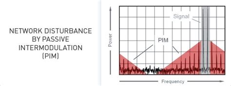
Passive intermodulation (PIM) is a form of interference that occurs in passive components of a wireless communication system when two or more high-power signals are present. PIM is caused by the nonlinear mixing of these signals, resulting in the generation of unwanted intermodulation products that can interfere with the desired signals.
In the context of printed circuit boards (PCBs) used in 5G systems, PIM can be a significant problem. The high frequencies and power levels used in 5G networks make them particularly susceptible to PIM, which can degrade signal quality, reduce system capacity, and cause other performance issues.
Sources of PIM in PCBs
There are several potential sources of PIM in PCBs used in 5G systems:
-
Material non-linearities: The dielectric materials used in PCBs can exhibit non-linear behavior when subjected to high-power signals, leading to PIM.
-
Surface roughness: Rough surfaces on the PCB can cause signal reflections and scattering, which can contribute to PIM.
-
Connector interfaces: Poor connections or damaged connectors can cause PIM due to metal-to-metal contact or oxidation.
-
Solder joints: Improperly formed or damaged solder joints can be a source of PIM.
-
Defects: Manufacturing defects such as voids, cracks, or delamination can cause PIM in PCBs.
Mitigating PIM in PCBs for 5G Systems
To minimize the impact of PIM in PCBs used in 5G systems, designers must take several factors into consideration:
Material Selection
The choice of materials used in the PCB can have a significant impact on PIM performance. Low-loss, high-linearity materials such as polytetrafluoroethylene (PTFE) or hydrocarbon ceramic laminates are often used in high-frequency PCBs to reduce PIM.
| Material | Dielectric Constant | Dissipation Factor | PIM Performance |
|---|---|---|---|
| PTFE | 2.1 | 0.0002 | Excellent |
| Hydrocarbon Ceramic | 3.5 | 0.0015 | Very Good |
| FR-4 | 4.4 | 0.02 | Poor |
Surface Finish
The surface finish of the PCB can also affect PIM performance. Smooth, uniform surfaces help to reduce signal reflections and scattering that can contribute to PIM. Some common surface finishes used in high-frequency PCBs include:
- Immersion silver (IAg)
- Electroless nickel immersion gold (ENIG)
- Electroless nickel electroless palladium immersion gold (ENEPIG)
| Surface Finish | Thickness (μm) | Surface Roughness (μm) | PIM Performance |
|---|---|---|---|
| IAg | 0.1 – 0.3 | 0.1 – 0.3 | Very Good |
| ENIG | 3 – 6 | 0.2 – 0.5 | Good |
| ENEPIG | 3 – 6 | 0.2 – 0.5 | Good |
Connector Design
The design and selection of connectors used in the PCB are critical for minimizing PIM. Connectors should be designed with tight tolerances, smooth surfaces, and minimal metal-to-metal contact. Some strategies for reducing PIM in connectors include:
- Using non-metallic materials such as plastic or ceramic
- Applying conductive coatings to the connector surfaces
- Ensuring proper alignment and mating of connectors
- Regularly inspecting and cleaning connectors
Manufacturing Process Control
Strict control over the manufacturing process is essential for producing PCBs with low PIM. This includes:
- Controlling the lamination process to ensure uniform bonding and minimal voids or delamination
- Using precision drilling and routing techniques to create smooth, burr-free holes and edges
- Implementing rigorous quality control measures to identify and reject defective boards
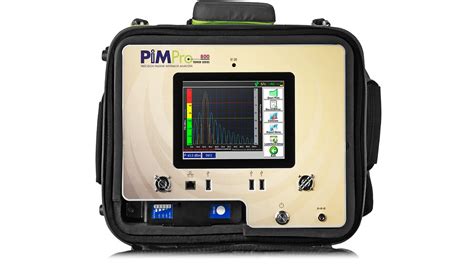
Testing for PIM in PCBs
To ensure that PCBs meet the stringent PIM requirements of 5G systems, thorough testing is necessary. PIM testing involves applying two or more high-power signals to the PCB and measuring the resulting intermodulation products.
PIM Test Setup
A typical PIM test setup consists of the following components:
- Signal generators to produce the high-power test signals
- A combiner to combine the test signals
- A directional coupler to inject the test signals into the PCB and to measure the reflected signals
- A spectrum analyzer to measure the intermodulation products
- A load or termination to absorb the transmitted signals
PIM Test Procedure
The PIM test procedure typically involves the following steps:
- Calibrate the test equipment to ensure accurate measurements.
- Connect the PCB to the test setup using appropriate adapters and cables.
- Apply the high-power test signals to the PCB at the desired frequencies and power levels.
- Measure the intermodulation products using the spectrum analyzer.
- Compare the measured PIM levels to the specified limits to determine if the PCB passes or fails the test.
PIM Test Limits
The acceptable PIM levels for a PCB depend on the specific application and the requirements of the 5G system. Typical PIM test limits for 5G PCBs are in the range of -153 dBc to -165 dBc, relative to the power of the test signals.
| Application | Frequency Range | PIM Test Limit |
|---|---|---|
| Sub-6 GHz 5G | 3.3 – 4.2 GHz | -153 dBc |
| mmWave 5G | 24.25 – 52.6 GHz | -165 dBc |

Frequently Asked Questions (FAQ)
1. What is the difference between passive and active intermodulation?
Passive intermodulation occurs in passive components such as connectors, cables, and PCBs, while active intermodulation occurs in active components such as amplifiers and mixers. Passive intermodulation is caused by the non-linear behavior of materials and surfaces, while active intermodulation is caused by the non-linear characteristics of active devices.
2. Can PIM be completely eliminated in PCBs?
While it is not possible to completely eliminate PIM in PCBs, it can be minimized through careful design, material selection, and manufacturing process control. By following best practices and thorough testing, PCBs can be produced with PIM levels that meet the requirements of 5G systems.
3. How does PIM affect 5G system performance?
PIM can have a significant impact on the performance of 5G systems. It can cause interference with the desired signals, reducing signal quality and system capacity. PIM can also increase the noise floor, making it more difficult to detect weak signals and reducing the overall sensitivity of the system.
4. What are the most critical factors in designing PCBs for low PIM?
The most critical factors in designing PCBs for low PIM are material selection, surface finish, connector design, and manufacturing process control. By using low-loss, high-linearity materials, smooth surfaces, well-designed connectors, and strict process control, PCBs can be produced with minimal PIM.
5. How often should PIM testing be performed on PCBs?
The frequency of PIM testing depends on the specific application and the requirements of the 5G system. In general, PIM testing should be performed on a sample of PCBs from each manufacturing lot to ensure consistent quality. Additional testing may be necessary if changes are made to the design, materials, or manufacturing process. Regular PIM testing can help to identify and correct issues before they impact system performance in the field.
No responses yet