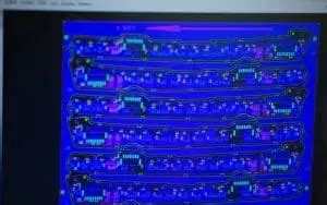
What is Panelization PCB?
Panelization PCB, also known as PCB array or PCB panel, is a process of grouping multiple printed circuit board designs onto a single panel for manufacturing. This technique is widely used in the electronics industry to increase production efficiency, reduce costs, and improve the overall quality of the PCBs.
Benefits of Panelization PCB
- Increased production efficiency
- Reduced manufacturing costs
- Improved quality control
- Simplified handling and assembly
The Panelization PCB Process
Step 1: PCB Design
The first step in the panelization process is to design the individual PCBs that will be grouped onto the panel. This involves creating the schematic, laying out the components, and routing the traces. The design should be optimized for panelization, taking into account factors such as:
- Board size and shape
- Component placement
- Trace routing
- Clearance between boards
Step 2: Panel Layout
Once the individual PCB designs are complete, they are arranged onto a single panel. The panel layout should consider the following:
- Number of boards per panel
- Spacing between boards
- Tooling holes and fiducial markers
- Panel material and thickness
Common Panel Layouts
| Layout | Description | Advantages | Disadvantages |
|---|---|---|---|
| Grid | Boards arranged in a regular grid pattern | Easy to layout, maximizes panel utilization | May require more tooling holes |
| Staggered | Boards arranged in an offset pattern | Reduces waste material, allows for more boards per panel | More complex to layout |
| Custom | Boards arranged in a custom pattern | Optimized for specific requirements | Requires more design effort |
Step 3: Tooling and Fiducial Markers
Tooling holes and fiducial markers are added to the panel to facilitate the manufacturing process. Tooling holes are used to secure the panel during drilling and routing, while fiducial markers provide reference points for automated assembly equipment.
Step 4: Panelization
The panelization process involves creating the panel design file, which includes the individual PCB designs, panel layout, and tooling information. This file is then sent to the PCB manufacturer for fabrication.
Step 5: Fabrication
The PCB manufacturer fabricates the panel according to the provided design file. This involves the following steps:
- Printing the circuit pattern onto the panel material
- Drilling holes for components and vias
- Plating the holes and traces
- Applying solder mask and silkscreen
- Testing and inspecting the panel
Step 6: Depanelization
After fabrication, the individual PCBs are separated from the panel through a process called depanelization. This can be done using various methods, such as:
- V-scoring
- Tab routing
- Perforating
- Laser cutting
The choice of depanelization method depends on factors such as board size, material, and required edge quality.
Panelization PCB Design Considerations
When designing PCBs for panelization, there are several key factors to consider:
Board Size and Shape
The size and shape of the individual PCBs should be optimized for panelization. Rectangular boards are easier to arrange on a panel than irregular shapes. The board dimensions should also allow for sufficient spacing between boards and tooling holes.
Component Placement
Components should be placed on the PCB in a way that minimizes the required board area and allows for efficient panelization. This may involve orienting components to fit within the available space and avoiding placing components too close to the board edges.
Trace Routing
Traces should be routed in a way that allows for clean separation of the individual boards during depanelization. This may involve adding additional space between traces near the board edges and avoiding routing traces too close to the board outline.
Material Selection
The choice of PCB material can impact the panelization process. Some materials, such as high-density interconnect (HDI) boards, may require special considerations for panelization due to their unique properties.

FAQ
1. What is the minimum spacing between boards on a panel?
The minimum spacing between boards depends on the specific manufacturing capabilities of the PCB fabricator. Generally, a minimum spacing of 2-3 mm is recommended, but it is best to consult with the manufacturer for their specific requirements.
2. Can different PCB designs be panelized together?
Yes, different PCB designs can be panelized together on the same panel, as long as they share the same material, thickness, and layer count. This can help to further reduce manufacturing costs and increase efficiency.
3. What is the maximum panel size?
The maximum panel size depends on the capabilities of the PCB manufacturer. Common panel sizes include 18″ x 24″ (457 mm x 610 mm) and 21″ x 24″ (533 mm x 610 mm), but larger sizes may be available from some manufacturers.
4. How does panelization affect PCB cost?
Panelization can significantly reduce the cost of PCB manufacturing by increasing production efficiency and reducing material waste. By grouping multiple boards onto a single panel, the fixed costs associated with setup and tooling are spread across a larger number of boards, resulting in a lower cost per board.
5. What are the challenges associated with panelization?
Some challenges associated with panelization include:
- Ensuring adequate spacing between boards
- Minimizing material waste
- Designing for efficient depanelization
- Maintaining consistent quality across all boards on the panel
By carefully considering these factors during the design and panelization process, these challenges can be effectively mitigated.
Conclusion
Panelization PCB is a critical process in the electronics manufacturing industry, offering numerous benefits such as increased efficiency, reduced costs, and improved quality control. By understanding the key steps and considerations involved in panelization, designers and manufacturers can optimize their PCB designs for successful panel fabrication and assembly.

No responses yet