Introduction to Solder Paste Stencils
Solder paste stencils are essential tools in the surface mount technology (SMT) assembly process. They are used to apply solder paste onto printed circuit boards (PCBs) with high precision and consistency. A well-designed solder paste stencil ensures the right amount of solder paste is deposited on the PCB pads, leading to reliable solder joints and minimizing defects such as solder bridges, insufficient solder, or solder beading.
However, designing an optimal solder paste stencil is not a straightforward task. It requires careful consideration of various factors, such as aperture size, shape, and orientation, as well as the stencil thickness and material. Improper stencil design can result in solder paste shortages, which can cause open circuits, poor solder joint formation, and reduced reliability of the assembled PCBs.
In this article, we will discuss the paint by numbers approach to solder paste stencil design, providing guidelines to help reduce solder paste shortages and improve the overall quality of the SMT assembly process.
Importance of Solder Paste Stencil Design
The solder paste stencil design plays a crucial role in determining the quality and reliability of solder joints in SMT assembly. A well-designed stencil should achieve the following objectives:
- Deposit the appropriate amount of solder paste on PCB pads
- Ensure consistent solder paste volume across all pads
- Minimize solder paste defects, such as bridging or insufficient solder
- Accommodate various component sizes and pitch requirements
- Facilitate easy and accurate alignment of the stencil with the PCB
Failing to meet these objectives can lead to solder paste shortages, which can cause a range of issues in the assembled PCBs, such as:
- Open circuits due to insufficient solder
- Weak or unreliable solder joints
- Inconsistent solder joint appearance
- Difficulty in achieving proper component placement
- Increased rework and repair costs
Therefore, it is essential to follow best practices and guidelines when designing solder paste stencils to minimize the risk of solder paste shortages and ensure high-quality SMT assembly.
Factors Affecting Solder Paste Stencil Design
Aperture Size and Shape
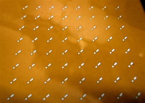
One of the primary factors influencing solder paste stencil design is the aperture size and shape. Apertures are the openings in the stencil through which solder paste is deposited onto the PCB pads. The size and shape of the apertures determine the volume and distribution of solder paste on the pads.
Aperture Size
The aperture size should be selected based on the dimensions of the PCB pads and the desired solder paste volume. As a general rule, the aperture size should be slightly larger than the PCB pad to ensure sufficient solder paste coverage. However, if the aperture size is too large, it can lead to excessive solder paste deposition, resulting in solder bridging or solder balling.
Aperture size is typically expressed as a percentage of the PCB pad size. For example, a 1:1 ratio means the aperture size is equal to the pad size, while a 1.2:1 ratio indicates the aperture is 20% larger than the pad.
Here are some general guidelines for selecting aperture sizes based on component pitch:
| Pitch (mm) | Aperture Size (% of pad size) |
|---|---|
| ≥ 0.65 | 100-110% |
| 0.5 – 0.65 | 110-120% |
| 0.4 – 0.5 | 120-130% |
| < 0.4 | 130-150% |
It is important to note that these are general guidelines, and the actual aperture size may need to be adjusted based on factors such as the solder paste type, PCB surface finish, and component geometry.
Aperture Shape
The shape of the aperture can also influence the solder paste deposition and the resulting solder joint quality. The most common aperture shapes are square, rectangular, and circular.
-
Square apertures are the most widely used and are suitable for most SMD pads. They provide good solder paste coverage and are easy to manufacture.
-
Rectangular apertures are used for elongated pads, such as those found on chip resistors or capacitors. They help ensure even solder paste distribution along the length of the pad.
-
Circular apertures are less common but can be used for round pads or BGA (Ball Grid Array) components. They can help reduce solder paste wastage and improve solder ball formation.
In some cases, custom aperture shapes may be required to accommodate unique component geometries or to address specific solder paste deposition challenges. For example, home plate or D-shaped apertures can be used for QFN (Quad Flat No-lead) or DFN (Dual Flat No-lead) packages to prevent solder bridging between the thermal pad and the adjacent pads.
Stencil Thickness
Stencil thickness is another critical factor in solder paste stencil design. The thickness of the stencil determines the volume of solder paste deposited on the PCB pads. A thicker stencil will deposit more solder paste, while a thinner stencil will deposit less.
The choice of stencil thickness depends on several factors, such as the component pitch, package type, and solder paste properties. In general, thinner stencils (0.1 mm to 0.15 mm) are used for fine-pitch components, while thicker stencils (0.15 mm to 0.2 mm) are used for larger components or when more solder paste volume is required.
Here are some guidelines for selecting stencil thickness based on component pitch:
| Pitch (mm) | Stencil Thickness (mm) |
|---|---|
| ≥ 0.65 | 0.15 – 0.2 |
| 0.5 – 0.65 | 0.125 – 0.15 |
| 0.4 – 0.5 | 0.1 – 0.125 |
| < 0.4 | 0.08 – 0.1 |
It is important to note that using a stencil that is too thick can lead to excessive solder paste deposition, resulting in solder bridging or tombstoning of components. On the other hand, using a stencil that is too thin can cause insufficient solder paste deposition, leading to open circuits or weak solder joints.
In some cases, a step stencil may be used to accommodate components with varying heights or to optimize solder paste deposition for different component types. A step stencil has different thicknesses in different areas, allowing for more precise control over solder paste volume.
Stencil Material
The choice of stencil material can also impact the solder paste deposition process and the resulting solder joint quality. The most common stencil materials are stainless steel, nickel-plated stainless steel, and laser-cut polyimide.
-
Stainless steel stencils are the most widely used and offer good durability, stability, and precision. They are suitable for high-volume production and can withstand multiple cleaning cycles.
-
Nickel-plated stainless steel stencils provide improved solder paste release and are less prone to solder paste adhesion. They are particularly useful for fine-pitch applications and can help reduce solder paste bridging.
-
Laser-cut polyimide stencils are a lower-cost alternative to metal stencils and are suitable for prototyping or low-volume production. They offer good flexibility and can conform to slightly uneven PCB surfaces. However, they have limited durability and may not be suitable for high-volume manufacturing.
The choice of stencil material depends on factors such as the production volume, component pitch, solder paste type, and budget constraints. It is essential to select a material that offers the right balance of precision, durability, and cost for the specific application.
Solder Paste Stencil Design Guidelines
Aperture Design
- Aperture Size:
- Ensure aperture sizes are appropriate for the component pitch and PCB pad dimensions.
- Use the guidelines provided in the “Aperture Size and Shape” section to select the appropriate aperture size.
-
Consider the solder paste type and PCB surface finish when determining the aperture size.
-
Aperture Shape:
- Use square apertures for most SMD pads.
- Use rectangular apertures for elongated pads, such as those found on chip resistors or capacitors.
- Consider circular apertures for round pads or BGA components.
-
Use custom aperture shapes, such as home plate or D-shaped apertures, for specific component types or to address solder paste deposition challenges.
-
Aperture Orientation:
- Orient apertures to match the orientation of the PCB pads.
- For rectangular pads, align the longer dimension of the aperture with the longer dimension of the pad.
-
For polarized components, such as tantalum capacitors or diodes, orient the aperture to match the component polarity.
-
Aperture Pitch:
- Ensure the pitch between apertures matches the pitch of the PCB pads.
- For fine-pitch components, consider using a stencil with a smaller aperture pitch to improve solder paste deposition accuracy.
Stencil Thickness Selection
-
Use the guidelines provided in the “Stencil Thickness” section to select the appropriate stencil thickness based on the component pitch.
-
Consider using a step stencil for PCBs with components of varying heights or to optimize solder paste deposition for different component types.
-
Evaluate the solder paste type and rheology when selecting the stencil thickness to ensure proper solder paste release and avoid defects such as solder bridging or insufficient solder.
Stencil Material Selection
-
Choose stainless steel stencils for high-volume production and applications requiring good durability and precision.
-
Consider nickel-plated stainless steel stencils for fine-pitch applications or when improved solder paste release is required.
-
Use laser-cut polyimide stencils for prototyping or low-volume production, where cost and flexibility are more important than durability.
Stencil Aperture Layout
-
Optimize the stencil aperture layout to ensure proper solder paste deposition and minimize the risk of solder paste shortages.
-
Avoid placing apertures too close to the edges of the stencil, as this can lead to solder paste smearing or inconsistent deposition.
-
Maintain a minimum distance between apertures to prevent solder paste bridging. The distance should be based on the component pitch and the solder paste type.
-
Consider the placement of fiducial marks on the stencil to aid in alignment with the PCB. Fiducial marks should be positioned in areas that do not interfere with solder paste deposition.
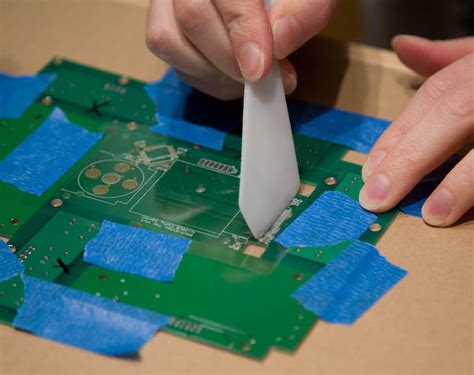
Stencil Cleaning and Maintenance
-
Regularly clean the solder paste stencil to remove any residual solder paste or debris that can affect the deposition process.
-
Use appropriate cleaning agents and methods based on the stencil material and the solder paste type.
-
Inspect the stencil for any damage, such as bent apertures or worn edges, and replace the stencil when necessary.
-
Store the stencil in a clean, dry environment to prevent contamination and ensure its longevity.

Solder Paste Selection and Printing Process
In addition to the solder paste stencil design, the choice of solder paste and the printing process parameters can also influence the occurrence of solder paste shortages. Here are some guidelines to consider:
- Solder Paste Selection:
- Choose a solder paste with the appropriate particle size and rheology for the specific application and stencil design.
- Consider the solder paste’s printing and reflow characteristics to ensure good printability and wetting.
-
Select a solder paste with good stability and shelf life to maintain consistent performance over time.
-
Printing Process Parameters:
- Optimize the print speed, pressure, and separation speed to achieve consistent solder paste deposition and minimize defects.
- Control the printer’s squeegee angle, pressure, and material to ensure proper solder paste transfer through the stencil apertures.
-
Maintain a consistent print environment, including temperature and humidity, to avoid variations in solder paste performance.
-
Printer Maintenance:
- Regularly clean and maintain the solder paste printer to ensure consistent performance and minimize the risk of contamination.
- Calibrate the printer’s alignment and pressure settings periodically to maintain accurate solder paste deposition.
Frequently Asked Questions (FAQ)
- What is the most common cause of solder paste shortages in SMT assembly?
-
The most common cause of solder paste shortages is improper solder paste stencil design. This can include incorrect aperture sizes, shapes, or orientation, as well as inappropriate stencil thickness or material selection.
-
How can I determine the appropriate aperture size for my components?
-
Aperture size is typically based on the component pitch and the PCB pad dimensions. Use the guidelines provided in the “Aperture Size and Shape” section of this article to select the appropriate aperture size for your components. Additionally, consider the solder paste type and PCB surface finish when making your decision.
-
When should I use a step stencil instead of a standard stencil?
-
A step stencil is useful when your PCB has components of varying heights or when you need to optimize solder paste deposition for different component types. By having different stencil thicknesses in different areas, you can better control the solder paste volume for each component type.
-
How often should I clean my solder paste stencil?
-
The frequency of stencil cleaning depends on factors such as the solder paste type, production volume, and environmental conditions. As a general rule, it is recommended to clean the stencil after every shift or when you notice any signs of solder paste buildup or contamination. Regular cleaning helps maintain consistent solder paste deposition and reduces the risk of defects.
-
Can solder paste selection impact the occurrence of solder paste shortages?
- Yes, solder paste selection can influence the occurrence of solder paste shortages. Choosing a solder paste with the appropriate particle size, rheology, and printing characteristics for your specific application and stencil design can help minimize the risk of shortages. Additionally, using a solder paste with good stability and shelf life can ensure consistent performance over time.
Conclusion
Solder paste stencil design plays a critical role in achieving high-quality solder joints and minimizing solder paste shortages in SMT assembly. By following the paint by numbers approach and adhering to the guidelines discussed in this article, you can optimize your stencil design for your specific components and manufacturing requirements.
Remember to consider factors such as aperture size, shape, and orientation, as well as stencil thickness and material when designing your stencil. Additionally, pay attention to the solder paste selection and printing process parameters to ensure consistent solder paste deposition and minimize defects.
Regular stencil cleaning and maintenance, as well as proper storage, are also essential for maintaining consistent solder paste deposition and reducing the risk of shortages.
By implementing these guidelines and best practices, you can improve the reliability and quality of your SMT assembly process, reducing rework and repair costs while increasing customer satisfaction.
No responses yet