Introduction to PCB Design and PADS Software
Printed Circuit Board (PCB) design is a crucial aspect of electronic product development. It involves creating a layout of electronic components and the connections between them on a board. PADS is a powerful PCB design software that offers a comprehensive set of tools for designing and verifying PCBs. In this tutorial, we will guide you through the process of designing a PCB using PADS software.
What is PCB Design?
PCB design is the process of creating a layout of electronic components and the connections between them on a printed circuit board. The layout is then used to manufacture the physical board. PCB design involves several steps, including schematic capture, component placement, routing, and verification.
Why Use PADS for PCB Design?
PADS is a popular PCB design software that offers a range of features and tools for designing and verifying PCBs. Some of the benefits of using PADS include:
- Intuitive user interface
- Powerful schematic capture and layout tools
- Advanced routing and placement capabilities
- Comprehensive library of components
- Integration with other design tools and manufacturing processes
Getting Started with PADS
System Requirements
Before you start using PADS, make sure your system meets the following requirements:
| Operating System | Processor | RAM | Hard Disk Space |
|---|---|---|---|
| Windows 10 | Intel Core i5 or higher | 8 GB or more | 20 GB or more |
Installing PADS
To install PADS, follow these steps:
- Download the PADS installer from the official website.
- Run the installer and follow the on-screen instructions.
- Activate your license by entering the license key provided by the vendor.
- Launch PADS and create a new project.

Creating a Schematic in PADS
What is a Schematic?
A schematic is a graphical representation of an electronic circuit. It shows the components and the connections between them using symbols and lines. Creating a schematic is the first step in PCB design.
Creating a New Schematic
To create a new schematic in PADS, follow these steps:
- In the PADS main window, click on “File” and then “New”.
- Select “Schematic” from the list of options and click “OK”.
- Enter a name for your schematic and click “OK”.
Adding Components to the Schematic
To add components to your schematic, follow these steps:
- Click on the “Place” menu and select “Component”.
- In the component library, search for the component you want to add.
- Click on the component to select it and then click on the schematic to place it.
- Repeat steps 2-3 for all the components you want to add.
Connecting Components
To connect components in your schematic, follow these steps:
- Click on the “Place” menu and select “Wire”.
- Click on the first component you want to connect.
- Click on the second component you want to connect.
- Repeat steps 2-3 for all the connections you want to make.

Creating a PCB Layout in PADS
What is a PCB Layout?
A PCB layout is a physical representation of the schematic. It shows the actual placement of components on the board and the routing of connections between them. Creating a PCB layout is the next step after creating a schematic.
Creating a New PCB Layout
To create a new PCB layout in PADS, follow these steps:
- In the PADS main window, click on “File” and then “New”.
- Select “PCB” from the list of options and click “OK”.
- Enter a name for your PCB layout and click “OK”.
Placing Components on the PCB
To place components on your PCB layout, follow these steps:
- In the schematic window, select the components you want to place on the PCB.
- Click on the “Tools” menu and select “Create PCB”.
- In the PCB layout window, arrange the components as desired.
- Use the “Move” tool to adjust the position of components if needed.
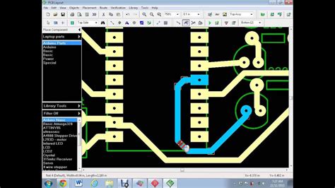
Routing Connections on the PCB
To route connections on your PCB layout, follow these steps:
- Click on the “Route” menu and select “Interactive Routing”.
- Click on the first pad you want to connect.
- Click on the second pad you want to connect.
- Repeat steps 2-3 for all the connections you want to make.
- Use the “Edit” tool to adjust the routing if needed.

Verifying and Finalizing the PCB Design
Design Rule Check (DRC)
Design Rule Check (DRC) is a process of verifying that your PCB design meets the manufacturing requirements and design rules. To run a DRC in PADS, follow these steps:
- Click on the “Tools” menu and select “DRC”.
- Select the design rules you want to check and click “OK”.
- Review the DRC report and fix any errors or warnings.
Generating Manufacturing Files
Once your PCB design is verified and finalized, you need to generate manufacturing files for production. To generate manufacturing files in PADS, follow these steps:
- Click on the “File” menu and select “Fabrication Outputs”.
- Select the output format and options you want and click “OK”.
- Save the output files in a desired location.
Frequently Asked Questions (FAQ)
- What is the difference between a schematic and a PCB layout?
-
A schematic is a graphical representation of an electronic circuit, while a PCB layout is a physical representation of the schematic on a printed circuit board.
-
Can I create a PCB layout without a schematic?
-
While it is possible to create a PCB layout without a schematic, it is not recommended. A schematic helps you visualize the circuit and catch errors early in the design process.
-
What is the purpose of Design Rule Check (DRC)?
-
DRC is a process of verifying that your PCB design meets the manufacturing requirements and design rules. It helps identify and fix errors before sending the design for production.
-
What are the different output files generated for PCB manufacturing?
-
The common output files generated for PCB manufacturing include Gerber files, drill files, and pick and place files.
-
Can I import a schematic from another design tool into PADS?
- Yes, PADS supports importing schematics from various design tools using standard file formats such as EDIF and DXF.
Conclusion
PCB design is a critical aspect of electronic product development, and PADS is a powerful tool for designing and verifying PCBs. In this tutorial, we covered the basics of PCB design using PADS, including creating a schematic, placing components, routing connections, and verifying the design. By following these steps and best practices, you can create high-quality PCB designs efficiently and effectively.
No responses yet