Introduction to Pad Stack Design for Fine Pitch Components
In the world of electronics manufacturing, pad stack design plays a crucial role in ensuring the reliability and functionality of printed circuit boards (PCBs), especially when dealing with fine pitch components. As technology advances and devices become more compact, designers face the challenge of accommodating smaller components with tighter spacing. This article delves into the intricacies of pad stack design for fine pitch components, providing insights and best practices to help you navigate this complex aspect of PCB design.
What is Pad Stack Design?
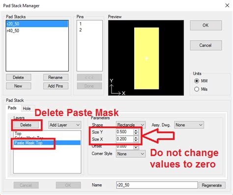
Pad stack design refers to the process of defining the shape, size, and arrangement of pads on a PCB. A pad is a conductive area on the PCB surface where a component lead or pin is soldered. The pad stack encompasses all the layers of the PCB, including the copper layers, solder mask, and surface finish. Proper pad stack design ensures reliable electrical connections, mechanical stability, and manufacturability of the PCB.
Challenges of Fine Pitch Components
Fine pitch components, such as Ball Grid Arrays (BGAs), Quad Flat Pack (QFP), and Quad Flat No-Lead (QFN) packages, pose unique challenges for pad stack design. These components have small lead pitches, typically ranging from 0.4mm to 0.8mm, which requires precise alignment and tight tolerances. Some of the challenges associated with fine pitch components include:
- Limited space for routing traces between pads
- Increased risk of solder bridging and short circuits
- Difficulty in achieving reliable solder joints
- Stringent manufacturing and assembly requirements
To overcome these challenges, designers must carefully consider various aspects of pad stack design, such as pad size, shape, and spacing.
Pad Size and Shape Considerations
Pad Size
Determining the appropriate pad size is crucial for fine pitch components. The pad size should be large enough to accommodate the component lead or pin, while also providing sufficient area for a reliable solder joint. However, oversized pads can lead to solder bridging and reduce the available space for routing traces. The pad size is typically calculated based on the component’s lead pitch and the PCB manufacturing capabilities.
Here’s a table showing recommended pad sizes for common fine pitch components:
| Component Type | Lead Pitch (mm) | Recommended Pad Size (mm) |
|---|---|---|
| QFP | 0.5 | 0.3 x 0.7 |
| QFN | 0.5 | 0.3 x 0.3 |
| BGA | 0.8 | 0.5 (diameter) |
Pad Shape
The shape of the pad can also impact the reliability and manufacturability of the solder joint. Common pad shapes for fine pitch components include:
- Rectangular pads: Offer a larger surface area for soldering and are suitable for QFP and QFN packages.
- Circular pads: Commonly used for BGA packages and provide a uniform solder joint.
- Oblong pads: A combination of rectangular and circular pads, offering the benefits of both shapes.
Designers should consider the component package and the assembly process when selecting the appropriate pad shape.

Pad Spacing and Pitch Considerations
Pad Spacing
Pad spacing refers to the distance between adjacent pads on the PCB. For fine pitch components, the pad spacing is determined by the lead pitch of the component. Adequate pad spacing is essential to prevent solder bridging and short circuits. The minimum pad spacing is dictated by the PCB manufacturing capabilities and the assembly process.
Here’s a table showing recommended minimum pad spacing for different lead pitches:
| Lead Pitch (mm) | Minimum Pad Spacing (mm) |
|---|---|
| 0.4 | 0.2 |
| 0.5 | 0.25 |
| 0.8 | 0.4 |
Pitch Considerations
In addition to pad spacing, designers must also consider the pitch of the component leads. The pitch is the distance between the centers of adjacent leads. Fine pitch components have smaller pitches, which requires precise alignment during the assembly process. Misalignment can lead to solder bridging and open circuits.
To ensure proper alignment, designers should incorporate fiducial marks on the PCB. Fiducial marks are reference points that help align the component leads with the pads during the pick-and-place process. They are typically placed near the corners of the component footprint.

Solder Mask and Surface Finish
Solder Mask
Solder mask is a protective layer applied over the copper traces on the PCB, leaving only the pads exposed for soldering. For fine pitch components, the solder mask design is critical to prevent solder bridging and ensure reliable solder joints. The solder mask opening should be slightly larger than the pad size to accommodate the solder paste and prevent solder from spreading to adjacent pads.
Here’s a table showing recommended solder mask openings for different pad sizes:
| Pad Size (mm) | Solder Mask Opening (mm) |
|---|---|
| 0.3 x 0.7 | 0.4 x 0.8 |
| 0.3 x 0.3 | 0.4 x 0.4 |
| 0.5 (diameter) | 0.6 (diameter) |
Surface Finish
The surface finish on the pads plays a crucial role in ensuring reliable solder joints. Common surface finishes for fine pitch components include:
- Immersion silver (IAg)
- Electroless nickel immersion gold (ENIG)
- Organic solderability preservative (OSP)
Each surface finish has its advantages and disadvantages in terms of cost, shelf life, and solderability. Designers should consider the component requirements and the assembly process when selecting the appropriate surface finish.

Design for Manufacturability (DFM)
DFM Guidelines
Design for Manufacturability (DFM) is an approach that considers the manufacturing process during the design phase to ensure the PCB can be efficiently and reliably manufactured. For fine pitch components, DFM guidelines help minimize manufacturing defects and improve yield. Some key DFM guidelines for pad stack design include:
- Adhere to the minimum pad size and spacing requirements
- Use consistent pad shapes and sizes for similar components
- Provide adequate clearance between pads and adjacent traces
- Incorporate fiducial marks for accurate component placement
- Follow the recommended solder mask opening guidelines
By following DFM guidelines, designers can reduce manufacturing costs, improve quality, and accelerate time-to-market.
Collaboration with Manufacturing Partners
Collaborating with PCB manufacturing partners is essential for successful pad stack design. Manufacturers have experience and expertise in dealing with fine pitch components and can provide valuable insights and recommendations. Designers should engage with manufacturers early in the design process to ensure the pad stack design is compatible with their manufacturing capabilities and assembly processes.
Regular communication and feedback between designers and manufacturers can help identify and resolve any potential issues before the PCB enters production. This collaboration can lead to improved design quality, reduced manufacturing costs, and faster time-to-market.
Frequently Asked Questions (FAQ)
- What is the minimum pad size for a 0.5mm pitch QFP component?
-
The recommended pad size for a 0.5mm pitch QFP component is 0.3mm x 0.7mm.
-
How can I prevent solder bridging between pads of fine pitch components?
-
To prevent solder bridging, ensure adequate pad spacing based on the lead pitch, use appropriate solder mask openings, and follow DFM guidelines for pad stack design.
-
What is the purpose of fiducial marks in pad stack design?
-
Fiducial marks serve as reference points to align the component leads with the pads during the pick-and-place assembly process, ensuring accurate component placement.
-
Can I use the same pad stack design for different surface finishes?
-
While the basic pad stack design can be similar, the specific requirements for pad size, shape, and solder mask opening may vary depending on the chosen surface finish. It’s essential to consult with your manufacturing partner to ensure compatibility.
-
How can collaborating with PCB manufacturers improve my pad stack design?
- PCB manufacturers have expertise in dealing with fine pitch components and can provide valuable insights and recommendations to optimize your pad stack design for manufacturability. Collaborating early in the design process can help identify and resolve potential issues, leading to improved design quality and reduced manufacturing costs.
Conclusion
Pad stack design for fine pitch components is a critical aspect of PCB design that requires careful consideration of various factors, including pad size, shape, spacing, solder mask, and surface finish. By understanding the challenges and best practices associated with fine pitch components, designers can create reliable and manufacturable PCBs.
Adhering to DFM guidelines and collaborating with PCB manufacturing partners are essential for successful pad stack design. This approach ensures that the PCB can be efficiently manufactured, minimizes the risk of defects, and reduces overall costs.
As technology continues to advance and components become smaller, the importance of proper pad stack design will only increase. By staying informed about the latest techniques and best practices, designers can navigate the complexities of fine pitch components and create PCBs that meet the demands of modern electronics.

No responses yet