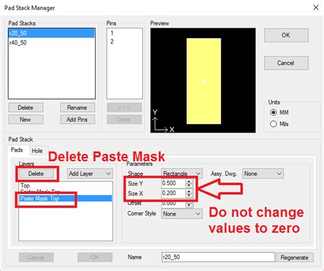
Introduction to Pad stack design
Pad stack design is a critical aspect of printed circuit board (PCB) design, as it plays a vital role in ensuring the reliability and functionality of the final product. A pad stack refers to the combination of copper pads, drilled holes, and other features that form the connection point between a component and the PCB. Proper pad stack design is essential for achieving optimal electrical, thermal, and mechanical performance of the PCB.
In this article, we will dive deep into the intricacies of pad stack design and the fabrication process. We will explore the various factors that influence pad stack design, industry standards, and best practices to follow. Additionally, we will discuss the fabrication process and the challenges associated with manufacturing pad stacks.
Factors Influencing Pad Stack Design
Several factors must be considered when designing pad stacks for a PCB. These factors include:
Component Requirements
The pad stack design must accommodate the specific requirements of the components being used. This includes the package type, pin count, pitch, and size. For example, surface mount devices (SMDs) require different pad stack designs compared to through-hole components.
PCB Fabrication Capabilities
The PCB fabrication process imposes certain limitations on pad stack design. Factors such as the minimum drill hole size, copper thickness, and annular ring requirements must be taken into account. The fabrication capabilities of the chosen PCB manufacturer should be considered during the design phase.
Electrical Requirements
Pad stack design affects the electrical performance of the PCB. The size and shape of the pads, as well as the spacing between them, impact impedance, signal integrity, and current-carrying capacity. Designers must ensure that the pad stacks meet the electrical requirements of the circuit.
Thermal Management
Thermal management is another crucial aspect of pad stack design. The pad stacks must be designed to efficiently dissipate heat generated by the components. This is particularly important for high-power devices such as power transistors and voltage regulators.
Mechanical Stability
Pad stacks play a role in the mechanical stability of the PCB assembly. They must be designed to withstand the stresses and strains encountered during the assembly process and in the final application. Proper pad stack design helps prevent issues such as pad lifting, solder joint failures, and component misalignment.

Industry Standards for Pad Stack Design
Several industry standards provide guidelines and recommendations for pad stack design. These standards ensure consistency, reliability, and compatibility across different PCB designs and manufacturers. Some of the key standards include:
IPC-7351B
IPC-7351B is a widely adopted standard for pad stack design. It provides guidelines for land pattern geometries, solder mask openings, and courtyard dimensions for various component types and package styles. This standard helps designers create pad stacks that are compatible with industry-standard component footprints.
IPC-2221A
IPC-2221A is a general standard for PCB design. It includes recommendations for pad stack design, such as minimum annular ring requirements, hole sizes, and pad-to-hole ratios. This standard ensures that pad stacks meet the necessary electrical and mechanical requirements.
IPC-2222A
IPC-2222A is a sectional standard that focuses on rigid organic printed boards. It provides guidelines for pad stack design specific to rigid PCBs, including recommendations for copper foil thickness, hole wall plating, and via design.

Best Practices for Pad Stack Design
To ensure optimal pad stack design, designers should follow these best practices:
-
Adhere to industry standards: Follow the guidelines provided by relevant industry standards such as IPC-7351B, IPC-2221A, and IPC-2222A. These standards ensure compatibility and reliability of the pad stacks.
-
Consider component requirements: Design pad stacks based on the specific requirements of the components being used. Consult component datasheets and application notes for recommended pad sizes and shapes.
-
Account for fabrication capabilities: Ensure that the pad stack design is compatible with the capabilities of the chosen PCB fabrication process. Communicate with the PCB manufacturer to understand their specific requirements and limitations.
-
Optimize for electrical performance: Design pad stacks to meet the electrical requirements of the circuit. Consider factors such as impedance matching, signal integrity, and current-carrying capacity when determining pad sizes and spacing.
-
Ensure proper thermal management: Incorporate thermal management considerations into the pad stack design. Use thermal vias and appropriate pad sizes to facilitate heat dissipation from power-hungry components.
-
Maintain mechanical stability: Design pad stacks to withstand mechanical stresses during assembly and operation. Adhere to minimum annular ring requirements and ensure adequate pad-to-hole ratios to prevent pad lifting and solder joint failures.
-
Perform design reviews: Conduct thorough design reviews to catch any potential issues with the pad stack design. Use design rule checks (DRC) and other validation tools to ensure compliance with industry standards and manufacturing constraints.

Pad Stack Fabrication Process
The fabrication process for pad stacks involves several steps that are critical to ensuring the quality and reliability of the final PCB. The main steps in the pad stack fabrication process include:
Drilling
The first step in pad stack fabrication is drilling the holes. The holes are drilled according to the specified sizes and locations in the PCB design files. High-precision drilling machines are used to ensure accurate hole placement and diameters.
Plating
After drilling, the holes are plated with a conductive material, typically copper. The plating process involves depositing a thin layer of copper on the walls of the drilled holes. This plating ensures reliable electrical connection between the layers of the PCB.
Copper Patterning
Once the holes are plated, the copper layers of the PCB are patterned according to the design files. This process involves selectively removing unwanted copper to create the desired pad shapes and traces. Photolithography and etching techniques are commonly used for copper patterning.
Solder Mask Application
Solder mask is a protective coating applied to the PCB surface, leaving only the exposed pads and other areas that require soldering. The solder mask helps prevent solder bridging and short circuits during the assembly process. It also provides insulation and protection for the copper traces.
Surface Finish
The final step in pad stack fabrication is the application of a surface finish. The surface finish is a thin layer of material, such as gold, silver, or organic solderability preservative (OSP), applied to the exposed pads. The surface finish enhances solderability, prevents oxidation, and improves the reliability of the solder joints.
Challenges in Pad Stack Fabrication
Pad stack fabrication can present several challenges that must be addressed to ensure the quality and reliability of the final PCB. Some of the common challenges include:
Hole Wall Quality
Ensuring the quality of the hole walls is critical for reliable electrical connections. Issues such as rough hole walls, smear, and debris can compromise the plating process and lead to poor electrical performance. Proper drilling parameters and cleaning processes must be employed to maintain hole wall quality.
Annular Ring Breakout
Annular ring breakout occurs when the copper pad around a drilled hole is not adequately supported, resulting in the pad lifting or separating from the PCB surface. This issue can be caused by improper pad stack design, manufacturing defects, or excessive mechanical stress. Adhering to minimum annular ring requirements and proper design practices can help prevent annular ring breakout.
Plating Uniformity
Achieving uniform plating thickness in the holes is essential for reliable electrical connections. Uneven plating can lead to poor signal integrity and increased resistance. Proper control of the plating process parameters, such as current density and solution composition, is necessary to ensure plating uniformity.
Solder Mask Registration
Accurate registration of the solder mask to the copper pads is crucial for proper soldering and component placement. Misaligned solder mask can result in exposed copper, solder bridging, or insufficient solder coverage. Precise alignment and imaging techniques are required to achieve accurate solder mask registration.
Frequently Asked Questions (FAQ)
-
What is a pad stack in PCB design?
A pad stack refers to the combination of copper pads, drilled holes, and other features that form the connection point between a component and the PCB. It includes the pad size, shape, and layer stack-up information. -
Why is pad stack design important?
Proper pad stack design is crucial for ensuring the electrical, thermal, and mechanical performance of the PCB. It affects signal integrity, heat dissipation, and the reliability of solder joints. Poor pad stack design can lead to manufacturing defects and component failures. -
What are the key factors to consider when designing pad stacks?
When designing pad stacks, designers must consider factors such as component requirements, PCB fabrication capabilities, electrical requirements, thermal management, and mechanical stability. These factors influence the size, shape, and spacing of the pads, as well as the hole sizes and plating specifications. -
What industry standards provide guidelines for pad stack design?
Several industry standards, such as IPC-7351B, IPC-2221A, and IPC-2222A, provide guidelines and recommendations for pad stack design. These standards ensure consistency, reliability, and compatibility across different PCB designs and manufacturers. -
What are some common challenges in pad stack fabrication?
Common challenges in pad stack fabrication include ensuring hole wall quality, preventing annular ring breakout, achieving uniform plating thickness, and maintaining accurate solder mask registration. These challenges require careful control of manufacturing processes and adherence to design guidelines to ensure the quality and reliability of the final PCB.
| Component Package | Pad Size (mm) | Hole Size (mm) | Pitch (mm) |
|---|---|---|---|
| SOIC-8 | 1.50 x 0.60 | 0.80 | 1.27 |
| QFP-64 | 1.00 x 0.50 | 0.30 | 0.50 |
| BGA-256 | 0.50 x 0.50 | – | 1.00 |
| TO-220 | 2.50 x 2.50 | 1.50 | 2.54 |
Table 1: Example pad stack dimensions for common component packages
Conclusion
Pad stack design and fabrication are critical aspects of PCB design and manufacturing. Proper pad stack design ensures optimal electrical, thermal, and mechanical performance of the PCB, while the fabrication process brings the design to life. Designers must consider various factors, adhere to industry standards, and follow best practices to create reliable and manufacturable pad stacks.
Understanding the challenges associated with pad stack fabrication, such as hole wall quality, annular ring breakout, plating uniformity, and solder mask registration, is essential for designing PCBs that can be manufactured effectively. Close collaboration between designers and PCB manufacturers is necessary to ensure the successful realization of the pad stack design.
By mastering the intricacies of pad stack design and fabrication, PCB designers can create high-quality, reliable, and cost-effective products that meet the ever-increasing demands of modern electronics. In the next part of this series, we will delve deeper into advanced pad stack design techniques and explore case studies to illustrate the practical application of these concepts.

No responses yet