Introduction to Microvia PCB Technology
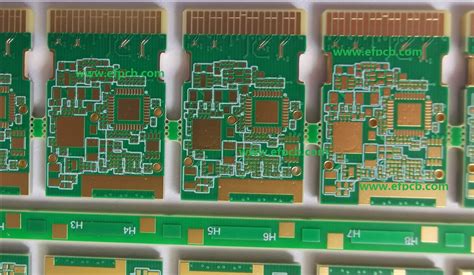
Microvia PCB technology has revolutionized the electronics industry by enabling the creation of high-density interconnect (HDI) printed circuit boards. These PCBs feature microvias, which are small, laser-drilled holes that allow for the connection of multiple layers within the board. Microvia PCBs offer numerous benefits, including reduced board size, improved signal integrity, and enhanced reliability.
What are Microvias?
Microvias are tiny, laser-drilled holes that are typically less than 150 microns (0.15 mm) in diameter. They are used to connect the outer layers of a PCB to the inner layers, allowing for a higher density of interconnections. Microvias can be stacked, staggered, or filled with conductive material to create complex, multi-layer PCB designs.
Advantages of Microvia PCB Technology
- Reduced board size and weight
- Improved signal integrity and reduced noise
- Enhanced reliability and durability
- Increased design flexibility and functionality
- Cost-effective for high-volume production
Microvia PCB Design Considerations
When designing a microvia PCB, several key factors must be considered to ensure optimal performance and manufacturability.
Layer Stack-up
The layer stack-up of a microvia PCB is crucial to its performance and manufacturability. A typical microvia PCB stack-up may include the following layers:
| Layer | Description |
|---|---|
| Top Layer | Signal layer with microvias |
| Ground Layer | Provides shielding and reduces noise |
| Signal Layers | Inner layers for signal routing |
| Power Layer | Distributes power to components |
| Bottom Layer | Signal layer with microvias |
Via Types and Placement
Microvias can be classified into three main types based on their placement and function:
- Blind vias: Connect an outer layer to an inner layer
- Buried vias: Connect inner layers without reaching the outer layers
- Through vias: Connect all layers of the PCB
When placing vias, designers must consider the following factors:
- Via size and pitch
- Via-to-pad and via-to-trace clearance
- Via fill material (copper, conductive paste, or epoxy)
Signal Integrity and Impedance Control
Maintaining signal integrity and controlling impedance are critical aspects of microvia PCB design. Designers must consider the following factors:
- Trace width and spacing
- Dielectric material properties
- Characteristic impedance of traces
- Termination and matching networks
Design for Manufacturability (DFM)
Designing a microvia PCB with manufacturability in mind is essential for ensuring a successful, cost-effective production process. Key DFM considerations include:
- Minimum feature sizes (traces, spaces, and vias)
- Copper balance and distribution
- Solder mask and silkscreen design
- Panelization and routing

Microvia PCB Manufacturing Process
The manufacturing process for microvia PCBs involves several specialized steps that differ from traditional PCB fabrication.
Laser Drilling
Microvias are created using laser drilling, which involves using a high-powered laser to create tiny, precise holes in the PCB substrate. The two main types of lasers used for microvia drilling are:
- CO2 lasers: Used for larger microvias (100-150 microns)
- UV lasers: Used for smaller microvias (50-100 microns)
Plating and Filling
After laser drilling, the microvias are plated with a conductive material, typically copper, to create an electrical connection between layers. The plating process involves the following steps:
- Desmear: Removing debris and preparing the via surface
- Electroless copper deposition: Creating a thin, conductive seed layer
- Electrolytic copper plating: Building up the copper thickness
In some cases, microvias may be filled with a conductive paste or epoxy to improve reliability and prevent air entrapment.
Lamination and Bonding
The individual layers of a microvia PCB are laminated together using heat and pressure. The lamination process involves the following steps:
- Aligning the layers
- Applying prepreg (pre-impregnated) material between layers
- Pressing the stack-up in a hot press
- Curing the resin to bond the layers together
Imaging and Etching
The outer layers of the microvia PCB are imaged and etched using standard photolithography and chemical etching processes. This involves:
- Applying a photoresist coating
- Exposing the resist to UV light through a photomask
- Developing the resist to reveal the desired circuit pattern
- Etching away the unwanted copper
- Stripping the remaining resist

Cost Considerations for Microvia PCBs
The cost of manufacturing microvia PCBs is generally higher than that of traditional PCBs due to the specialized equipment and processes involved. However, the total cost of ownership (TCO) can be lower for microvia PCBs when considering factors such as:
- Reduced board size and material usage
- Improved yield and reliability
- Faster time-to-market
- Lower assembly and rework costs
Factors Affecting Microvia PCB Cost
Several factors can influence the cost of manufacturing microvia PCBs:
- Board size and complexity
- Number of layers and microvias
- Material selection (substrate, copper, solder mask)
- Surface finish (HASL, ENIG, OSP)
- Quantity and production volume
Cost Optimization Strategies
To optimize the cost of microvia PCBs, designers and manufacturers can employ the following strategies:
- Minimizing board size and layer count
- Standardizing materials and processes
- Optimizing panel utilization and routing
- Leveraging economies of scale for high-volume production
- Collaborating with experienced microvia PCB manufacturers

Frequently Asked Questions (FAQ)
- What is the minimum size of a microvia?
-
The minimum size of a microvia depends on the laser technology used. UV lasers can produce microvias as small as 50 microns, while CO2 lasers typically create microvias between 100 and 150 microns.
-
Can microvias be stacked?
-
Yes, microvias can be stacked to create connections between multiple layers. Stacked microvias are drilled and plated sequentially, with each new via connecting to the previous one.
-
What materials are used for microvia PCBs?
-
Microvia PCBs typically use high-performance substrate materials such as FR-4, polyimide, or PTFE (Teflon). The choice of material depends on the application, operating conditions, and required electrical properties.
-
How do microvia PCBs differ from HDI PCBs?
-
Microvia PCBs are a type of HDI (High-Density Interconnect) PCB that specifically use microvias for layer-to-layer connections. HDI PCBs may also incorporate other features such as fine-pitch components, embedded passives, or advanced packaging techniques.
-
Are microvia PCBs suitable for all applications?
- Microvia PCBs are particularly well-suited for applications that require high component density, compact form factors, and high-speed signal transmission. However, they may not be necessary or cost-effective for simpler, low-density designs. The decision to use microvia technology should be based on the specific requirements and constraints of each project.
Conclusion
Microvia PCB technology offers numerous benefits for modern electronics, enabling the creation of high-density, high-performance designs in compact form factors. By understanding the design considerations, manufacturing processes, and cost factors associated with microvia PCBs, engineers and managers can make informed decisions when developing new products.
As the demand for smaller, faster, and more reliable electronic devices continues to grow, microvia PCBs will play an increasingly important role in shaping the future of the industry. By staying up-to-date with the latest advancements in microvia technology and partnering with experienced manufacturers, companies can leverage the full potential of this innovative approach to PCB design and fabrication.
No responses yet