Introduction to PCB Manufacture
Printed Circuit Boards (PCBs) are the backbone of modern electronics. They provide a platform for mounting and interconnecting electronic components, allowing for the creation of complex circuits in a compact and efficient manner. PCB manufacture is a multi-step process that involves various techniques and materials to produce high-quality boards for a wide range of applications.
In this article, we will delve into the step-by-step process of PCB manufacture, covering everything from design and layout to fabrication and assembly. Whether you are an electronics enthusiast, a hobbyist, or a professional, understanding the PCB manufacturing process is essential for creating reliable and functional electronic devices.
PCB Design and Layout
Schematic Design
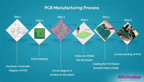
The first step in PCB manufacture is creating a schematic diagram of the electronic circuit. A schematic is a graphical representation of the circuit’s components and their interconnections. It serves as a blueprint for the PCB layout and helps in understanding the circuit’s functionality.
To create a schematic, designers use Electronic Design Automation (EDA) software such as KiCad, Eagle, or Altium Designer. These tools provide a user-friendly interface for placing components and drawing connections between them. The schematic should include all the necessary components, their values, and any special requirements, such as power supply voltages and current ratings.
PCB Layout
Once the schematic is complete, the next step is to create the PCB layout. The layout is a physical representation of the circuit on the PCB, showing the placement of components and the routing of traces (copper paths) that connect them.
PCB layout is a critical step in the manufacturing process as it directly affects the board’s performance, signal integrity, and manufacturability. Designers must consider factors such as component placement, trace width and spacing, via size and placement, and power and ground planes to ensure optimal functionality and reliability.
EDA software is used to create the PCB layout, allowing designers to import the schematic and place components on a virtual board. The software provides tools for routing traces, adding vias (holes that connect different layers), and defining the board’s outline and mounting holes.
Design Rule Check (DRC)
After completing the PCB layout, designers perform a Design Rule Check (DRC) to ensure that the layout meets the manufacturing requirements and design constraints. The DRC verifies that the layout adheres to the specified rules, such as minimum trace width, spacing between traces, and clearance between components.
The DRC helps identify potential issues that could lead to manufacturing defects or performance problems. By resolving these issues before sending the design for fabrication, designers can save time and costs associated with rework and redesign.
Gerber File Generation
The final step in the design phase is generating Gerber files. Gerber files are industry-standard file formats used to describe the PCB layout for manufacturing. They contain information about the copper layers, solder mask, silkscreen, and drill holes.
EDA software can generate Gerber files automatically based on the PCB layout. These files are then sent to the PCB manufacturer for fabrication.

PCB Fabrication
Board Material Selection
PCBs are typically made from a composite material called FR-4, which consists of a woven fiberglass fabric impregnated with an epoxy resin. FR-4 is the most common PCB material due to its excellent electrical, mechanical, and thermal properties.
Other PCB materials include:
- High-frequency materials (e.g., Rogers, Teflon) for RF and microwave applications
- Flexible materials (e.g., polyimide) for flexible PCBs
- Metal core materials (e.g., aluminum) for high-power LED applications
The choice of PCB material depends on the specific requirements of the application, such as operating frequency, temperature range, and mechanical
constraints.
Copper Clad Laminate
The first step in PCB fabrication is preparing the copper-clad laminate (CCL). The CCL consists of a thin layer of Copper Foil bonded to one or both sides of the insulating substrate material (e.g., FR-4).
The thickness of the copper foil is specified in ounces per square foot (oz/ft²). Common copper weights include 0.5 oz/ft², 1 oz/ft², and 2 oz/ft². Thicker copper is used for high-current applications, while thinner copper is suitable for fine-pitch designs.
Drilling
After preparing the CCL, the next step is drilling holes for through-hole components and vias. Drilling is performed using high-speed CNC drilling machines equipped with small-diameter drill bits.
The drill file, generated from the PCB layout, contains information about the size and location of each hole. The drilling machine uses this file to accurately position and drill the holes in the CCL.
Copper Patterning
Once the holes are drilled, the next step is to create the copper pattern on the PCB. This is done using a photolithography process, which involves the following steps:
- Applying a photosensitive resist layer to the copper surface
- Exposing the resist to UV light through a photomask (generated from the PCB layout)
- Developing the resist to remove the exposed areas
- Etching the exposed copper using a chemical etchant
- Stripping the remaining resist to reveal the final copper pattern
The photolithography process is repeated for each copper layer in the PCB.
Lamination
For multi-layer PCBs, the individual copper-patterned layers are laminated together using heat and pressure. The layers are aligned and stacked with prepreg (pre-impregnated) material between them. Prepreg is a partially cured B-stage epoxy that acts as an insulating layer and bonds the copper layers together.
The stacked layers are then placed in a lamination press, where they are subjected to high temperature and pressure to cure the prepreg and bond the layers together.
Solder Mask Application
After lamination, a solder mask layer is applied to the PCB surface. Solder mask is a protective coating that covers the copper traces, leaving only the exposed pads for component soldering.
Solder mask is typically applied using a screen printing process, followed by UV curing. The solder mask color is usually green but can be other colors such as black, white, or blue.
Silkscreen Printing
The final step in PCB fabrication is silkscreen printing. Silkscreen is a text and graphics layer printed on the PCB surface for component identification, branding, and assembly instructions.
Silkscreen is applied using a screen printing process, similar to solder mask application. The silkscreen ink is typically white but can be other colors for better visibility or aesthetic appeal.

PCB Assembly
Surface Mount Technology (SMT)
Surface Mount Technology (SMT) is the most common method for assembling components on a PCB. SMT involves placing components directly on the PCB surface and soldering them using a reflow oven.
The SMT assembly process includes the following steps:
- Solder paste application: A thin layer of solder paste is applied to the component pads using a stencil or screen printing process.
- Component placement: SMT Components are placed on the solder paste using a pick-and-place machine, which accurately positions the components based on the PCB layout.
- Reflow soldering: The PCB with the placed components is passed through a reflow oven, where the solder paste melts and forms a permanent connection between the components and the PCB pads.
- Inspection: After reflow soldering, the PCB is visually inspected for any defects or misaligned components.
Through-Hole Technology (THT)
Through-Hole Technology (THT) involves inserting component leads through drilled holes in the PCB and soldering them on the opposite side. THT is used for larger components, such as connectors and transformers, that require
mechanical strength and reliability.
The THT assembly process includes the following steps:
- Component insertion: THT components are manually or automatically inserted into the drilled holes on the PCB.
- Wave soldering: The PCB with the inserted components is passed over a wave of molten solder, which fills the holes and creates a connection between the component leads and the PCB.
- Inspection: After wave soldering, the PCB is visually inspected for any defects or poorly soldered joints.
Mixed Technology
Some PCBs require a combination of SMT and THT components. In such cases, the assembly process involves a mix of both technologies. Typically, SMT components are placed and reflowed first, followed by THT component insertion and wave soldering.

PCB Testing and Inspection
Automated Optical Inspection (AOI)
Automated Optical Inspection (AOI) is a machine vision-based technique used to inspect PCBs for manufacturing defects. AOI systems use high-resolution cameras and image processing algorithms to detect issues such as:
- Missing or misaligned components
- Solder bridges or shorts
- Insufficient or excessive solder
- Damaged or lifted pads
AOI is performed after SMT and THT assembly to identify defects early in the manufacturing process, reducing rework and scrap costs.
In-Circuit Testing (ICT)
In-Circuit Testing (ICT) is a method of testing the functionality of individual components on a PCB. ICT involves using a bed-of-nails fixture that makes contact with the PCB’s test points, allowing the tester to apply signals and measure responses from each component.
ICT can detect issues such as:
- Open or short circuits
- Incorrect component values
- Faulty or missing components
- Polarity errors
ICT is performed after AOI to ensure that the PCB is functionally correct before proceeding to the next stage of assembly or testing.
Functional Testing
Functional testing involves testing the PCB’s overall functionality and performance under simulated operating conditions. This type of testing verifies that the PCB meets the specified requirements and functions as intended in the final application.
Functional testing may include:
- Power-on testing
- Signal integrity testing
- Environmental testing (e.g., temperature, humidity, vibration)
- Burn-in testing
Functional testing is typically performed on a sample of PCBs from each manufacturing batch to ensure consistency and reliability.
PCB Finishing and Packaging
Surface Finish
After testing and inspection, the PCB undergoes a surface finish process to protect the exposed copper pads and improve solderability. Common surface finishes include:
- Hot Air Solder Leveling (HASL): A tin-lead alloy is applied to the pads and leveled using hot air.
- Electroless Nickel Immersion Gold (ENIG): A layer of nickel is deposited on the pads, followed by a thin layer of gold.
- Immersion Silver (IAg): A thin layer of silver is deposited on the pads.
- Organic Solderability Preservative (OSP): A thin, organic coating is applied to the pads to prevent oxidation.
The choice of surface finish depends on the application requirements, such as shelf life, solderability, and compatibility with the assembly process.
Electrical Test
A final electrical test, known as a “flying probe” test, may be performed on the finished PCB. This test uses movable probes to verify the continuity and isolation of the PCB’s traces and vias, ensuring that there are no short circuits or open connections.
Packaging and Shipping
After the surface finish and final testing, the PCBs are packaged for shipping. Packaging methods vary depending on the PCB’s size, quantity, and shipping requirements. Common packaging options include:
- Vacuum sealing: PCBs are sealed in moisture-barrier bags with desiccants to prevent moisture damage during storage and shipping.
- Tray
packaging: PCBs are placed in ESD (electrostatic discharge) safe trays, which are then stacked and secured in boxes for shipping.
– Reel packaging: Smaller PCBs, such as those for SMT assembly, may be packaged on reels for automated assembly processes.
The packaged PCBs are then shipped to the customer or the next stage of the product assembly process.
Frequently Asked Questions (FAQ)
1. What is the typical turnaround time for PCB manufacturing?
The turnaround time for PCB manufacturing varies depending on the complexity of the design, the PCB manufacturer’s capacity, and the shipping method. Typical turnaround times range from 24 hours for simple, quick-turn PCBs to 2-3 weeks for more complex, multi-layer designs.
2. What factors affect the cost of PCB manufacturing?
Several factors influence the cost of PCB manufacturing, including:
- PCB size and thickness
- Number of layers
- Quantity ordered
- Material type
- Surface finish
- Complexity of the design (e.g., small traces, tight clearances)
- Turnaround time
In general, larger quantities, simpler designs, and longer turnaround times result in lower costs per PCB.
3. What are the most common PCB manufacturing defects?
Some of the most common PCB manufacturing defects include:
- Solder bridges or shorts
- Open circuits
- Incorrect component placement
- Insufficient or excessive solder
- Delamination or voids in the PCB substrate
- Damaged or lifted pads
- Drill misalignment or incorrect hole sizes
Careful design, adherence to manufacturing guidelines, and thorough testing and inspection can help minimize these defects.
4. Can I manufacture PCBs at home?
Yes, it is possible to manufacture simple PCBs at home using a combination of manual and chemical processes. However, home PCB manufacturing is limited in terms of the complexity of the designs, the number of layers, and the overall quality and reliability of the finished boards. For more advanced designs or production-grade PCBs, it is recommended to use a professional PCB manufacturing service.
5. What is the difference between a prototype PCB and a production PCB?
Prototype PCBs are typically manufactured in small quantities (1-10 pieces) to test and validate the design before committing to a larger production run. They may be manufactured using different processes or materials compared to production PCBs to reduce costs and lead times.
Production PCBs are manufactured in larger quantities (100+ pieces) using optimized processes and materials for consistency, reliability, and cost-effectiveness. They undergo more rigorous testing and inspection to ensure they meet the required quality standards for the end application.
Conclusion
PCB manufacturing is a complex, multi-step process that involves a combination of design, fabrication, assembly, and testing techniques. By understanding the various stages of PCB manufacture, from schematic design to final packaging, engineers and technicians can optimize their designs for manufacturability, reliability, and cost-effectiveness.
As PCB technology continues to evolve, with smaller features, higher frequencies, and more advanced materials, the importance of a robust and well-controlled manufacturing process becomes even more critical. By staying up-to-date with the latest PCB manufacturing techniques and best practices, electronics professionals can ensure that their products meet the highest standards of quality and performance.
No responses yet