
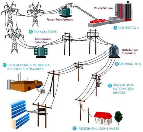
Why Power Distribution Matters for Reducing Noise and EMI
Proper power distribution is critical for minimizing noise and electromagnetic interference (EMI) in electronic systems. Noise on power rails can couple into sensitive analog circuitry and degrade performance. Switching currents from digital ICs can generate EMI that interferes with other circuits or exceeds regulatory limits.
Some key aspects of low noise, low EMI power distribution include:
- Using separate analog and digital power supplies to prevent digital noise from coupling into analog circuitry
- Proper bypassing and decoupling to provide a low impedance path for high frequency noise
- Minimizing power distribution network (PDN) impedance to prevent voltage fluctuations
- Reducing ground impedance and eliminating ground loops
- Filtering power supplies to attenuate conducted EMI
Let’s dive into each of these areas in more detail.
Separating Analog and Digital Power Supplies
One of the most effective ways to prevent digital noise from degrading analog performance is to use separate power supplies and ground returns for the analog and digital sections of a PCB. Digital ICs draw large switching currents which can generate significant amounts of high frequency noise on their power rails. If this noisy digital supply is shared with sensitive analog circuits, the noise can couple in and reduce dynamic range, increase jitter, and cause other issues.
Ideally, analog and digital circuitry should be partitioned onto separate PCBs with their own dedicated power supplies. If they must be integrated onto the same board, use separate supply rails and ground planes with filtering between the analog and digital sections. Never allow the analog and digital ground planes to overlap or directly connect – only join them at a single point, usually at the power supply.
Some mixed-signal ICs like ADCs and DACs have separate analog and digital supply pins for exactly this reason. Always honor this separation, providing clean analog supplies for the AVDD pins and digital supplies for the DVDD pins.
Proper Bypassing and Decoupling
All ICs, whether analog or digital, require proper bypassing and decoupling for stable operation. The goal is to provide a very low impedance path for high frequency noise and transients to get shunted to ground, preventing them from spreading throughout the power distribution network.
Bypassing is done at the IC level, with small ceramic capacitors (usually 0.1uF or less) placed very close to each power pin. The objective is to provide a local energy reservoir for fast switching transients. At high frequencies, a capacitor’s impedance is dominated by its equivalent series inductance (ESL). Minimizing trace length is critical to reduce ESL. For optimal bypassing:
- Place capacitors as close to IC power pins as possible, ideally < 1cm away
- Use wide, short traces or power/ground planes to connect capacitors
- Mount capacitors on the same side of the PCB as the IC to avoid vias
- Use small package sizes like 0402 or 0201 to minimize capacitor ESL
Decoupling is a board-level approach to reduce low frequency power supply impedance. Bulk decoupling capacitors, typically 1uF or greater, are distributed around the PCB to provide charge storage and limit voltage droops during switching transients. While electrolytic capacitors were traditionally used, polymer tantalum and ceramic technologies like MLCC are generally better choices today due to their much lower ESR.
Selecting the right amount of bypassing and decoupling capacitance requires knowing the dynamic current profile and min/max allowable voltage of each IC. Digital components like FPGAs and CPUs have particularly demanding transient current requirements. Carefully study the power sequencing and FPGA vendor guidelines to determine the PDN impedance target and amount of decoupling needed.

PDN Impedance and Ground Bounce
The power distribution network impedance must be kept low to maintain a stable supply voltage in the presence of constantly changing load currents. A significant component of PDN impedance is actually the ground (return) path. As high frequency currents flow through the ground impedance, voltage drops develop which can shift the “ground” reference significantly. This ground bounce can couple noise into signals referencing ground.
To minimize PDN impedance and ground bounce:
- Use thin dielectrics to create power/ground plane capacitance
- Avoid neck-down or cut-outs in ground planes that cause return path discontinuities
- Provide uninterrupted ground planes and use stitching vias to tie planes together
- Consider power plane islands for supplies driving heavy transient loads
Special consideration must be given to PDN impedance in mixed-signal designs with both analog and digital ICs. The noisy digital currents can bounce the digital ground, which can capacitively couple into the analog plane if they overlap. Either avoid overlapping analog/digital ground pours entirely, or place them on adjacent layers so they create an embedded capacitance that helps rather than hurts.
Ground Impedance and Loops
Improper grounding is a common source of noise issues in systems. High frequency return currents want to flow directly under their trace in the ground plane due to mutual inductance. If there is a discontinuity in the ground plane that interrupts this natural return path, the current must find another way to return to the source, often through a large loop area.
These ground loops act as antennas to efficiently radiate and pick up interference. Loops can also develop if different ground points in the system are at different potentials. Trying to force current to flow through ground paths with DC potential differences is a recipe for unwanted conducted noise.
To avoid ground impedance and loop issues:
- Eliminate ground plane splits or gaps that cause discontinuous return paths
- When a ground plane must be split, provide stitching capacitors to allow high frequency current to “jump” the gap
- Provide a single-point ground and avoid connecting different ground nets in multiple places
- Use star-point grounding and isolate noisy/quiet grounds to avoid large circulating currents
Mixed-signal PCBs require careful grounding. The analog and digital grounds should only join at one point, usually the power supply or the ADC/DAC itself. Connecting them in multiple spots allows noisy digital currents to flow through sensitive analog grounds.
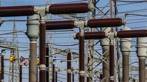
Power Supply Filtering
Switching power supplies are a common source of conducted EMI. Their fast rise/fall times and high switching frequencies can generate noise that spreads throughout the power distribution system. Linear regulators are usually much quieter, but are inefficient for large voltage drops and high current loads.
Filtering the output of switching power supplies is important to attenuate high frequency conducted EMI. A common filter topology is a multi-stage LC filter with a series ferrite choke to block high frequency noise and shunt capacitors to short it to ground. Resistors are sometimes added to create a pi filter for additional attenuation.
The table below shows some common power supply filter components and their properties:
| Component | value range | Impedance | Notes |
|---|---|---|---|
| Electrolytic cap | 1uF – 1000uF+ | Low Z at low freq | High ESR, used for bulk storage |
| Ceramic cap | 1nF – 10uF | Low Z at high freq | Use multiple small caps vs one large |
| Ferrite choke | 1uH – 100uH+ | High Z at high freq | Match impedance to circuit, rated for DC current |
| Resistors | 1-100 ohms | Constant Z | Power rating limits use to low current |
For very noise-sensitive analog supplies, further regulation and filtering may be needed beyond the initial power supply filter. Low-noise LDO linear regulators provide additional isolation from power supply noise, especially low frequency ripple. Ferrite beads in series with the LDO input/output help block any remaining high frequency noise.
PCB Layout Considerations
Proper PCB layout is essential for maintaining power integrity and minimizing EMI. Some key layout best practices include:
- Partition the board into analog/digital sections, each with their own supplies and ground pours
- Place switching regulators far from sensitive analog circuitry
- Route power traces on inner layers sandwiched between ground planes when possible
- Avoid crossing gaps or splits in ground planes with power traces
- Provide uninterrupted ground planes on adjacent layers
- Stitch ground planes together with closely-spaced vias near connectors and ICs
- Flood all unused areas of the PCB with ground copper to reduce impedance
- Keep ground return paths short and direct under signal traces
Bypass capacitor placement and routing is particularly important. Locate them as close as possible to IC power pins. Use large-width, short traces to minimize series inductance. Place vias tangent to pads to avoid blocking routes. Smaller package sizes like 0402 and 0201 have much lower ESL than larger packages.
When placing decoupling capacitors, focus on covering a broad range of frequencies. Use multiple smaller value caps in parallel instead one large value cap. A typical decoupling strategy uses bulk storage capacitors like 4.7uF near the voltage regulator, mid-size 0.1-1uF capacitors distributed throughout the PCB, and small 0.01uF bypass caps sprinkled very close to IC power pins.
Measuring and Characterizing the PDN
Designing a solid PDN involves both upfront analysis and post-layout verification. Early in the design process, hand calculations or SPICE simulations can be used to estimate the needed amount of decoupling to meet a target impedance. Capacitor vendors often provide tools to assist with selection and simulation of different decoupling options.
Post-layout PDN analysis is important to validate the impedance across frequency and identify problem areas. Most PCB tools include some form of PDN analysis to visualize current density and impedance. The PDN’s AC impedance can be measured directly on the prototype PCB by injecting a sinusoidal current and measuring the voltage ripple that develops.
More sophisticated PDN characterization techniques include:
- VNA (vector network analyzer) measurements with a 2-port pigtail setup
- TDR (time domain reflectometry) to measure plane impedance
- Near-field EMI scanning to identify current hotspots on the PCB
- 1-port resonance measurements to extract the PDN equivalent circuit
The ultimate validation of PDN and EMI performance must be done at the system level with the actual hardware. Careful probing of sensitive analog supplies can help identify any coupled digital noise. Dedicated EMI scanning tools or chambers allow the radiated and conducted emissions of the product to be thoroughly evaluated and compared against relevant regulatory limits.
FAQ
What is the most important factor for reducing power supply noise?
Minimizing PDN impedance is the single most important factor for reducing power supply noise. A low impedance PDN prevents voltage fluctuations in the presence of changing load currents. Use thin dielectrics, plenty of decoupling capacitance, and uninterrupted ground planes to keep PDN impedance low.
How much bypassing capacitance is needed per IC?
The amount of bypassing needed depends on the transient current profile and voltage tolerance of the IC. As a general rule of thumb, use about 0.01-0.1uF of ceramic bypassing per power pin, located as close as possible to the IC. Consult vendor datasheets and app notes for specific decoupling guidelines for power-hungry chips like FPGAs, CPUs, and ADCs.
What type of capacitors are best for decoupling?
MLCCs (multi-layer ceramic capacitors) are usually the best choice for decoupling. They have very low ESL and ESR, and come in a range of small package sizes. Use X7R or X5R dielectric formulations, which have good stability over temperature. Avoid Y5V and Z5U.
How can ground loops be prevented?
Provide a continuous, unbroken ground plane for return currents. Avoid splitting ground planes or routing signals over gaps/holes. If the ground plane must be split, stitch the sections together with closely spaced vias. Connect different ground nets in the system at a single point to avoid DC offset voltages that can drive circulating ground loop currents.
What causes radiated EMI and how can it be minimized?
Radiated EMI is caused by high frequency currents flowing through unintended antennas like cables, traces, and ground planes. Minimize the loop area enclosed by signal and return paths. Avoid discontinuities in return planes that force currents to take long, circuitous paths. Provide local bypassing to contain noisy switching currents. Use shielding to contain strong fields.
No responses yet