Introduction to Length Tuning PCBs
A length-tuning-pcb, also known as a tunable PCB or adjustable PCB, is a printed circuit board that allows for precise adjustments to the electrical length of transmission lines. This innovative technology is crucial in various applications, such as high-frequency electronics, telecommunications, and antenna systems, where the accurate control of signal propagation is essential for optimal performance.
What is a Length Tuning PCB?
A length tuning PCB is a specialized printed circuit board that incorporates adjustable elements, such as variable capacitors or inductors, to fine-tune the electrical length of transmission lines. By modifying the electrical length, engineers can ensure that signals propagate through the circuit with the desired phase and amplitude, minimizing signal distortion and improving overall system performance.
Importance of Length Tuning PCBs in High-Frequency Applications
In high-frequency applications, such as radio frequency (RF) circuits and microwave systems, the precise control of signal propagation is critical. At these frequencies, even small variations in the electrical length of transmission lines can lead to significant signal degradation, resulting in reduced system efficiency and reliability.
Length tuning PCBs address this challenge by providing a means to adjust the electrical length of transmission lines dynamically. By incorporating variable components, such as capacitors or inductors, engineers can optimize the signal path for specific frequencies and operating conditions, ensuring optimal performance across a wide range of scenarios.
Principles of Length Tuning PCBs
Transmission Line Theory
To understand the working principles of length tuning PCBs, it is essential to grasp the fundamentals of transmission line theory. A transmission line is a medium that guides the propagation of electromagnetic waves, such as electrical signals, from one point to another. In PCBs, transmission lines are typically implemented using conductive traces or microstrip lines.
The electrical length of a transmission line is determined by its physical length and the velocity of signal propagation through the medium. The velocity of propagation, in turn, depends on the dielectric constant of the substrate material and the geometry of the transmission line.
Impedance Matching and Reflection
Impedance matching is a crucial aspect of high-frequency circuit design. When a signal encounters a change in impedance along its path, a portion of the signal is reflected back towards the source, leading to signal distortion and power loss. To minimize reflections and ensure efficient signal transmission, it is necessary to maintain a consistent impedance throughout the transmission line.
Length tuning PCBs play a vital role in impedance matching by allowing engineers to adjust the electrical length of transmission lines to match the impedance of connected components. By minimizing impedance mismatches, length tuning PCBs help to reduce signal reflections and improve overall system performance.
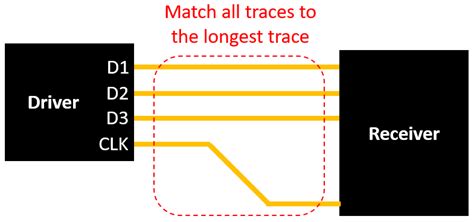
Phase Delay and Signal Synchronization
In complex high-frequency systems, such as phased array antennas or multi-channel communication systems, precise control over the phase delay of signals is essential for proper operation. Phase delay refers to the time difference between the input and output signals of a transmission line, and it is directly related to the electrical length of the line.
Length tuning PCBs enable engineers to adjust the phase delay of signals by modifying the electrical length of transmission lines. By ensuring that signals arrive at their destination with the desired phase relationship, length tuning PCBs facilitate signal synchronization and coherent combining, which are critical for applications such as beamforming and interference mitigation.
Design Considerations for Length Tuning PCBs
Substrate Material Selection
The choice of substrate material is a critical factor in the design of length tuning PCBs. The substrate material determines the dielectric constant and loss tangent of the PCB, which directly impact signal propagation and attenuation. Common substrate materials for high-frequency applications include:
- FR-4: A cost-effective and widely used substrate material, suitable for frequencies up to a few gigahertz.
- Rogers RO4000 series: Low-loss, high-performance substrates designed for microwave and millimeter-wave applications.
- Teflon-based substrates: Offer excellent electrical properties, including low dielectric constant and loss tangent, making them ideal for high-frequency applications.
When selecting a substrate material for a length tuning PCB, designers must consider factors such as the operating frequency range, environmental conditions, and cost constraints.
Tuning Element Selection
The choice of tuning elements is another crucial aspect of length tuning PCB design. Tuning elements are variable components that allow for the adjustment of the electrical length of transmission lines. The most common tuning elements used in length tuning PCBs are:
- Variable capacitors: Provide capacitive loading to the transmission line, allowing for fine-tuning of the electrical length.
- Variable inductors: Introduce inductive loading to the transmission line, enabling coarse adjustments to the electrical length.
- MEMS (Micro-Electro-Mechanical Systems) switches: Offer high-precision, low-loss switching capabilities for reconfigurable length tuning PCBs.
The selection of tuning elements depends on factors such as the required tuning range, resolution, and power handling capacity. Designers must also consider the integration of tuning elements into the PCB layout, ensuring proper placement and routing to minimize parasitic effects.
Electromagnetic Simulation and Optimization
Electromagnetic (EM) simulation plays a vital role in the design and optimization of length tuning PCBs. EM simulation tools, such as Ansys HFSS or Keysight ADS, allow designers to model and analyze the electrical behavior of the PCB, taking into account factors such as substrate properties, trace geometry, and component placement.
Through EM simulation, designers can optimize the PCB layout for desired performance characteristics, such as impedance matching, phase delay, and signal integrity. Iterative simulations and parameter sweeps enable designers to explore different tuning element configurations and optimize the design for specific operating conditions.

Applications of Length Tuning PCBs
Phased Array Antennas
Phased array antennas are a prime example of the application of length tuning PCBs. In a phased array antenna, multiple antenna elements are arranged in a grid-like pattern, and the relative phase of the signals feeding each element is adjusted to steer the antenna beam in a desired direction.
Length tuning PCBs are used to implement the phase shifters that control the relative phase of the signals feeding the antenna elements. By adjusting the electrical length of the transmission lines connecting the phase shifters to the antenna elements, designers can achieve precise beam steering and optimize antenna performance.
Wireless Communication Systems
Length tuning PCBs find extensive use in wireless communication systems, such as cellular networks, satellite communications, and Wi-Fi routers. In these applications, length tuning PCBs are employed to optimize signal transmission and reception, ensuring reliable and efficient communication.
For example, in a cellular base station, length tuning PCBs can be used to implement tunable filters and matching networks. By adjusting the electrical length of these components, engineers can optimize the system for specific frequency bands and minimize signal interference.
Test and Measurement Equipment
Length tuning PCBs are also used in test and measurement equipment, such as vector network analyzers (VNAs) and spectrum analyzers. In these applications, length tuning PCBs enable precise control over the electrical length of signal paths, ensuring accurate measurements and calibration.
For instance, in a VNA, length tuning PCBs can be used to implement tunable reference lines and calibration standards. By adjusting the electrical length of these components, engineers can compensate for cable delays and improve the accuracy of the measurement system.
Fabrication and Assembly of Length Tuning PCBs
PCB Manufacturing Process
The fabrication of length tuning PCBs follows a similar process to that of standard PCBs, with a few additional considerations. The key steps in the manufacturing process include:
- Substrate preparation: The chosen substrate material is cut to size and cleaned to remove any contaminants.
- Copper cladding: A layer of copper is laminated onto the substrate, forming the conductive layer for the PCB traces.
- Photolithography: The desired PCB pattern is transferred onto the copper layer using a photoresist and exposure to UV light.
- Etching: The unwanted copper is removed using a chemical etching process, leaving behind the desired traces and pads.
- Drilling: Holes are drilled through the PCB for component mounting and via connections.
- Plating: The drilled holes are plated with copper to establish electrical connections between layers.
- Solder mask and silkscreen: A protective solder mask is applied to the PCB, and a silkscreen layer is added for component labeling and identification.
When manufacturing length tuning PCBs, additional steps may be required to incorporate the tuning elements, such as variable capacitors or inductors. These components may be surface-mounted or embedded within the PCB substrate, depending on the specific design requirements.
Component Placement and Soldering
The placement and soldering of components on a length tuning PCB require special attention to ensure proper functionality and reliability. When placing tuning elements, designers must consider factors such as component orientation, proximity to other components, and potential interference.
Soldering techniques, such as reflow soldering or hand soldering, are used to attach the components to the PCB. Proper soldering is essential to establish reliable electrical connections and minimize signal loss. In some cases, specialized soldering techniques, such as low-temperature soldering or soldering under inert atmospheres, may be required to accommodate sensitive components or materials.
Testing and Validation
After fabrication and assembly, length tuning PCBs must undergo rigorous testing and validation to ensure they meet the desired performance specifications. Testing procedures may include:
- Visual inspection: A visual examination of the PCB to check for any manufacturing defects, such as poor soldering or damaged components.
- Electrical testing: Measurement of electrical characteristics, such as impedance, insertion loss, and phase delay, to verify that the PCB performs as expected.
- Functional testing: Evaluation of the PCB’s performance in its intended application, such as a phased array antenna or wireless communication system.
- Environmental testing: Exposure of the PCB to various environmental conditions, such as temperature extremes, humidity, and vibration, to assess its reliability and durability.
Validation of length tuning PCBs involves comparing the measured performance against the design specifications and making any necessary adjustments or optimizations. This iterative process ensures that the final product meets the required standards and can be reliably deployed in the intended application.
Future Trends and Developments
Advanced Materials and Manufacturing Techniques
As the demand for high-performance length tuning PCBs continues to grow, researchers and manufacturers are exploring advanced materials and manufacturing techniques to improve PCB performance and reliability. Some of the emerging trends in this area include:
- Low-loss substrate materials: The development of new substrate materials with lower dielectric loss and improved thermal stability, such as ceramic-filled PTFE or hydrocarbon ceramics, enables the design of length tuning PCBs for higher frequency applications.
- 3D printing: Additive manufacturing techniques, such as 3D printing, offer the potential for rapid prototyping and customization of length tuning PCBs. By printing the PCB structure and embedding tuning elements in a single process, designers can create complex, high-performance structures with reduced manufacturing time and cost.
- Embedded components: The integration of tuning elements directly into the PCB substrate, using techniques such as embedded capacitance or inductance, can lead to more compact and efficient designs. Embedded components also offer improved signal integrity and reduced parasitics compared to surface-mounted components.
Integration with Emerging Technologies
Length tuning PCBs are poised to play a crucial role in the development and deployment of emerging technologies, such as 5G wireless networks, Internet of Things (IoT) devices, and autonomous vehicles. As these technologies continue to evolve, the demand for high-performance, reconfigurable, and adaptive RF systems will drive the development of advanced length tuning PCB solutions.
For example, in 5G networks, length tuning PCBs can be used to implement agile antenna systems that can dynamically adapt to changing network conditions and user demands. In IoT devices, length tuning PCBs can enable compact, low-power, and multi-band RF front-ends for seamless connectivity across different wireless standards.
FAQ
- What is the main purpose of a length tuning PCB?
-
The main purpose of a length tuning PCB is to provide precise control over the electrical length of transmission lines, enabling optimization of signal propagation and system performance in high-frequency applications.
-
What are the common tuning elements used in length tuning PCBs?
-
Common tuning elements used in length tuning PCBs include variable capacitors, variable inductors, and MEMS switches. These elements allow for fine-tuning of the electrical length of transmission lines.
-
How does substrate material selection affect the performance of length tuning PCBs?
-
The choice of substrate material is critical in length tuning PCB design, as it determines the dielectric constant and loss tangent of the PCB. Low-loss, high-performance substrates, such as Rogers RO4000 series or Teflon-based substrates, are preferred for high-frequency applications to minimize signal attenuation and distortion.
-
What are some common applications of length tuning PCBs?
-
Length tuning PCBs find applications in various high-frequency systems, such as phased array antennas, wireless communication systems, and test and measurement equipment. They are used to optimize signal transmission, implement tunable filters and matching networks, and ensure accurate measurements and calibration.
-
What are some emerging trends in length tuning PCB technology?
- Some emerging trends in length tuning PCB technology include the development of advanced low-loss substrate materials, the use of 3D printing for rapid prototyping and customization, and the integration of embedded components for more compact and efficient designs. Additionally, length tuning PCBs are expected to play a crucial role in the development of emerging technologies, such as 5G networks and IoT devices.
No responses yet