What is an LED PCB?
An LED PCB, or light-emitting diode printed circuit board, is a specialized type of PCB designed to power and control LEDs. LEDs are highly efficient semiconductor devices that emit light when an electric current passes through them. By mounting LEDs onto a custom printed circuit board, they can be powered and their light output precisely controlled.
LED PCBs enable the use of LEDs for a wide range of lighting applications, including:
- Indicator lights on electronic devices
- Backlighting for LCD displays
- Architectural lighting
- Automotive lighting
- General illumination
Compared to traditional lighting technologies like incandescent and fluorescent, LEDs offer many advantages:
- Very high energy efficiency (more light output per watt)
- Extremely long lifespan (50,000+ hours)
- Compact size
- Directional light output
- Full color range and control
- Instant on/off switching
- Excellent durability
By integrating LEDs onto custom printed circuit boards, LED PCB assemblies maximize these inherent advantages of LEDs. They provide an optimized thermal and electrical environment to operate the LEDs while enabling intelligent control of the light output.
LED PCB Design Considerations
Designing an LED PCB involves careful consideration of the electrical, thermal, and optical requirements. The PCB must provide adequate power to the LEDs while managing heat dissipation. It also needs to enable the desired light output characteristics. Key design aspects include:
LED Type and Configuration
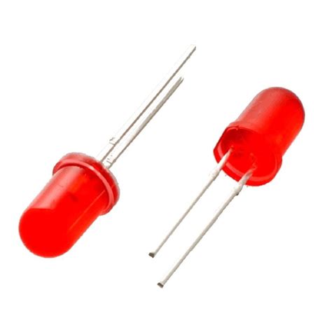
The type, quantity, and arrangement of LEDs on the PCB must be defined based on the target light output levels, efficacy, color, and directionality. LEDs are available in a range of packages, sizes, power ratings, and light colors.
Common LED package types used on PCBs include:
| Package | Description | Typical Power | Typical Applications |
|---|---|---|---|
| 5mm/T-1 3/4 | Cylindrical with domed lens | 0.1W | Indicator lights |
| 3mm/T-1 | Cylindrical with domed lens | 0.1W | Indicator lights |
| SMD 0402/0603/0805/1206 | Surface mount device | 0.1W | Backlighting, signage |
| High Power SMD | Surface mount, larger size | 1-5W | Illumination |
| COB (Chip-on-Board) | Multiple chips on ceramic substrate | 10-200W | High output lighting |
The schematic and PCB layout must be designed to connect the LEDs in the optimal electrical configuration, whether in parallel strings, series strings, or a matrix. Factors like target drive current, voltage drop, and power dissipation will determine the arrangement.
Drive Circuitry
LEDs are current-driven devices that require a constant DC current to operate optimally and consistently. The PCB must incorporate circuitry to regulate the current through the LEDs.
The most basic approach is to use a current-limiting resistor in series with the LEDs. However, this is inefficient and lacks performance. More sophisticated driver designs employ switching regulators or linear constant-current drivers to efficiently regulate the LED current.
The drive circuitry must be sized appropriately for the number and power of LEDs. It also needs to account for expected variations in the power supply voltage and LED forward voltage. Over-voltage and reverse polarity protection are important to include.
Heat Dissipation
While LEDs are highly efficient, they still dissipate a significant amount of heat, especially high power LEDs. Excess heat will degrade the LED performance and lifespan. Therefore, proper thermal management is critical for LED PCBs.
The PCB should be designed to conduct heat away from the LEDs to the ambient environment. This is typically accomplished by specifying a thermally-conductive PCB substrate material like metal-core PCB (MCPCB) or insulated metal substrate (IMS).
Thick copper layers and thermal vias can help transfer heat from the LED thermal pad to the PCB substrate. The PCB may also need to interface with an external heat sink to further aid cooling.
Thermal simulations using specialized PCB software can analyze the heat distribution and identify hot spots. The layout can then be optimized to minimize thermal issues.
Light Management
To achieve the desired light output profile, the PCB may need to incorporate secondary optics like reflectors and lenses. These can be mounted directly to the PCB near each LED to shape the light beam.
The placement of the LEDs and optics should be carefully considered relative to the product housing. Mechanical design collaboration is important to ensure the optimal light coupling and minimal losses.
If the LED PCB is used for backlighting, light diffusers and waveguides may be required to mix and distribute the light. These can be separate parts that interface with the PCB.
Control Features
Many LED applications require some form of control of the light intensity and/or color. This can range from simple on/off or dimming control to full color mixing and dynamic effects.
The PCB can include components like microcontrollers, driver ICs, sensors, and communication interfaces to enable these control features. Firmware must be developed to implement the control algorithms and functions.
Common control protocols for LED lighting include:
- 0-10V analog dimming
- PWM (Pulse Width Modulation) dimming
- DALI (Digital Addressable Lighting Interface)
- DMX512
- Bluetooth Low Energy
- Zigbee
The choice of control method depends on the application requirements, existing system interfaces, and cost targets.
Reliability Considerations
LED PCBs are often used in harsh operating environments with wide temperature ranges, moisture exposure, and vibration. Reliability is critical to ensure long operating life.
Proper component derating, materials selection, and assembly processes are important for reliability. Conformal coating can protect against moisture and contaminants. Strain relief should be applied to connectors and wiring.
Rigorous qualification testing, including accelerated life testing and environmental stress screening, should be performed to validate the design robustness. Field failure analysis and continuous improvement processes are also key.

LED PCB Manufacturing Process
The manufacturing process for LED PCBs follows the general PCB fabrication and assembly flow, with some specialized considerations for LEDs.
PCB Fabrication
-
Material Selection: LED PCBs typically use thermally-conductive base materials like MCPCB or IMS. FR-4 may be used for lower power designs.
-
Lamination: The base material is laminated with copper foil using heat and pressure. For MCPCB, a dielectric polymer layer is applied between the metal substrate and copper layer.
-
Photolithography: The copper layer is coated with a light-sensitive photoresist. The circuit pattern is transferred from a photomask to the photoresist by UV light exposure. The unexposed photoresist is then chemically removed.
-
Etching: The exposed copper is etched away using a chemical solution, leaving only the desired circuit traces.
-
Drilling: Holes are drilled through the PCB for vias, component leads, and mounting.
-
Plating: A thin layer of copper is electroplated onto the drilled hole walls to form plated through-holes. Additional copper may be plated on the traces for increased current capacity.
-
Soldermask: A polymer coating is applied to the PCB surface, excluding the component pads and exposed copper areas. This protects against solder bridging and corrosion.
-
Silkscreen: White ink is printed onto the soldermask to label components, pin 1 indicators, logos, and other markings.
-
Surface Finish: The exposed copper pads are coated with a surface finish to protect against oxidation and enhance solderability. Common finishes include HASL (hot air solder leveling), ENIG (electroless nickel immersion gold), and OSP (organic solderability preservative).
-
Electrical Test: The fabricated PCB is electrically tested for shorts and opens using flying probe or bed-of-nails testers.
PCB Assembly
-
Solder Paste Printing: A stainless steel stencil is aligned over the PCB and solder paste is spread across it, depositing paste on the component pads. The paste contains tiny solder spheres suspended in flux.
-
Component Placement: The PCB is loaded into a pick-and-place machine which uses vacuum nozzles to pick up components from feeders and place them onto the solder paste deposits. The placement force and time are carefully controlled for LEDs to avoid damage.
-
Reflow Soldering: The PCB with placed components travels through a reflow oven on a conveyor belt. The oven has multiple temperature zones which preheat, activate the flux, melt the solder, and cool the board. The activated flux removes oxides from the metals, allowing the solder to wet the surfaces and form reliable electrical and mechanical bonds.
-
Inspection: The assembled PCB is visually inspected, often with automated optical inspection (AOI) systems, to check for component presence, alignment, and solder defects. X-ray inspection may be used to examine solder joints hidden under components.
-
Rework and Repair: Any identified defects are reworked by manual soldering or component replacement.
-
Conformal Coating: For harsh environment applications, a thin polymer coating may be applied onto the assembled PCB to protect against moisture, dust, and contaminants.
-
Testing: The final assembly is functionally tested to verify proper operation of the LED circuitry and control features. This may involve powering up the board, measuring light output, and checking control functions. Automated test equipment (ATE) with custom test fixtures is often used for volume production.

Choosing an LED PCB Manufacturer
Selecting the right manufacturer is critical for a successful LED PCB project. Key factors to consider include:
Technical Capabilities
The manufacturer should have experience with LED PCBs and the specific technologies required for your design. This may include capabilities in thermal management, optical integration, and control systems.
Ask about their equipment and processes for PCB fabrication and assembly. Advanced capabilities like micro-vias, fine-pitch placement, and 3D AOI can enable more complex designs.
Quality Systems
The manufacturer should have a robust quality management system (QMS) in place, preferably certified to ISO 9001. They should also follow IPC standards for PCB fabrication and assembly.
Inquire about their defect tracking, corrective action, and continuous improvement processes. Regular quality audits and statistical process control (SPC) are important for consistent quality.
Supply Chain Management
The manufacturer’s ability to manage the supply chain is critical for timely delivery and cost control. They should have established relationships with reliable component suppliers, especially for LEDs and drivers.
Ask about their component sourcing, inventory management, and obsolescence management processes. They should be able to handle component lead times and shortages without impacting the project timeline.
Testing and Validation
Comprehensive testing and validation are essential for LED PCBs to ensure reliable performance in the end application. The manufacturer should have the necessary equipment and expertise to perform testing at various stages:
- Incoming component inspection and testing
- In-circuit testing (ICT) for shorts and opens
- Functional testing of the complete assembly
- Environmental testing (temperature, humidity, vibration)
- Accelerated life testing
- Light output and color measurement
Discuss the specific testing requirements for your project and how the manufacturer will meet them.
Cost and Lead Time
Of course, cost and lead time are important considerations for any PCB project. Get quotes from multiple manufacturers and compare the value they provide in terms of quality, reliability, and service.
However, be cautious about selecting the lowest bidder without considering the total cost of ownership. Cheaper upfront costs may be offset by higher defect rates, delays, or field failures.
Look for a manufacturer who can offer consistent pricing and lead times over the life of the project. They should also be able to handle volume ramp-up and provide cost reduction opportunities through design optimization and supply chain management.

Frequently Asked Questions (FAQ)
1. What are the advantages of LED PCBs over traditional lighting technologies?
LED PCBs offer several advantages over traditional lighting technologies like incandescent and fluorescent:
- Higher energy efficiency (more light output per watt of power)
- Longer lifespan (50,000+ hours)
- Smaller size and weight
- Directionality of light output
- Full color range and control
- Instant on/off switching
- Better durability and vibration resistance
These advantages make LED PCBs ideal for a wide range of applications, from indicator lights to general illumination.
2. What is a metal-core PCB (MCPCB) and why is it used for LED PCBs?
A metal-core PCB (MCPCB) is a type of PCB that uses a metal substrate, typically aluminum, as the base material instead of traditional FR-4. The metal substrate is laminated with a thin dielectric layer and copper circuit layer.
MCPCBs are commonly used for LED PCBs because of their excellent thermal conductivity. The metal substrate helps to quickly spread and dissipate the heat generated by the LEDs, which is critical for maintaining their performance and lifespan. This allows high power LEDs to be used in more compact designs without overheating.
3. How do I select the right LED for my PCB design?
Selecting the right LED depends on several factors:
- Required light output (lumens) and efficacy (lumens per watt)
- Target color (white, monochromatic, RGB) and color temperature for white LEDs
- Viewing angle and beam pattern
- Size and power constraints of the PCB
- Operating environment (temperature, humidity, vibration)
- Cost and availability
Start by defining the optical and electrical requirements for your application. Then, search for LEDs that meet those requirements from reputable manufacturers. Pay attention to the LED binning and color consistency specifications.
It’s also important to consider the LED package type and size, as this will impact the PCB layout and assembly process. Some common package types for PCB mounting include SMD, high-power SMD, and COB.
Finally, make sure to select an LED that can be reliably sourced and has a long-term availability commitment from the manufacturer. This is especially important for products with a long lifecycle.
4. What are some common challenges in LED PCB design and how can they be mitigated?
LED PCB design presents several challenges that must be carefully addressed:
-
Thermal management: LEDs generate a significant amount of heat that must be dissipated to maintain their performance and lifespan. This can be mitigated by using thermally-conductive PCB materials like MCPCB, providing adequate copper coverage and thickness, and incorporating thermal vias and external heatsinks.
-
Electrical driver design: LEDs require constant current drivers to maintain consistent light output. The driver circuit must be carefully designed to provide the optimal current level, regulate against variations in voltage, and protect against overcurrent and reverse polarity. This can be achieved through proper component selection, circuit simulation, and testing.
-
Optical integration: Achieving the desired light output pattern and uniformity can be challenging, especially for large arrays or edge-lit designs. This can be mitigated by using secondary optics like lenses and reflectors, as well as diffusers and waveguides for backlighting applications. Optical simulation software can also help optimize the design.
-
EMI and flicker: LED drivers can generate electromagnetic interference (EMI) and flicker if not properly designed. This can be mitigated by using appropriate filtering and shielding techniques, as well as selecting drivers with high PWM frequencies and/or linear current control.
-
Manufacturing and assembly: LED PCBs require specialized manufacturing processes and assembly techniques to ensure reliable bonding and avoid damaging the LEDs. This can be mitigated by selecting a manufacturer with experience in LED PCBs and following best practices for design for manufacturability (DFM) and design for assembly (DFA).
5. How do I ensure the reliability and longevity of my LED PCB in harsh environments?
Ensuring the reliability and longevity of LED PCBs in harsh environments requires careful design and testing:
- Use high-quality, automotive-grade components that are rated for the expected temperature range and have low failure rates.
- Follow best practices for PCB design, including proper component derating, copper sizing, and thermal management.
- Use conformal coating or encapsulation to protect against moisture, dust, and contaminants.
- Perform thorough testing and validation, including accelerated life testing, thermal cycling, and vibration testing.
- Implement robust quality control processes during manufacturing, such as X-ray inspection and burn-in testing.
- Monitor field performance and conduct failure analysis to identify and correct any design or manufacturing issues.
By taking a comprehensive approach to design, manufacturing, and testing, LED PCBs can be made highly reliable and long-lasting, even in demanding environments.
No responses yet