Introduction to KiCAD and Rayming
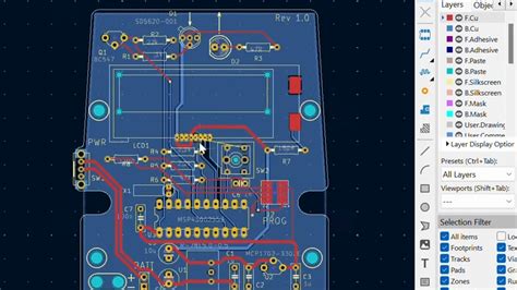
KiCAD is a popular open-source Electronic Design automation (EDA) software that allows users to design printed circuit boards (PCBs) from schematic capture to PCB Layout. It has gained a significant following among hobbyists, students, and professionals due to its powerful features and free availability.
Rayming, on the other hand, is a company that specializes in PCB manufacturing and assembly services. They have recently introduced a new feature that enables their systems to read native KiCAD data directly, streamlining the PCB Fabrication process for KiCAD users.
Benefits of KiCAD-Rayming Integration
The integration of KiCAD and Rayming brings several benefits to PCB Designers and manufacturers:
-
Seamless Data Transfer: With Rayming’s ability to read native KiCAD data, designers can directly send their KiCAD project files to Rayming without the need for intermediate file formats like Gerber or ODB++. This eliminates the potential for data loss or compatibility issues during file conversion.
-
Faster Turnaround Times: By eliminating the need for file conversion, the KiCAD-Rayming integration speeds up the PCB fabrication process. Designers can submit their KiCAD projects directly to Rayming, reducing the time spent on preparing and sending manufacturing data.
-
Improved Design Integrity: When using intermediate file formats, there is a risk of losing important design information or introducing errors during the conversion process. With Rayming’s ability to read native KiCAD data, the design integrity is maintained throughout the manufacturing process, ensuring that the manufactured PCBs match the original design intent.
-
Enhanced Collaboration: The KiCAD-Rayming integration facilitates better collaboration between PCB designers and manufacturers. Designers can communicate their design requirements and constraints directly within the KiCAD environment, and Rayming can provide feedback and suggestions based on their manufacturing capabilities and guidelines.

How KiCAD-Rayming Integration Works
The KiCAD-Rayming integration leverages the native file format used by KiCAD, which is the KiCAD project file (.kicad_pcb). This file contains all the necessary information about the PCB design, including the schematic, component footprints, board layout, and design rules.
When a designer is ready to manufacture their PCB, they can simply send the KiCAD project file directly to Rayming. Rayming’s systems are equipped to read and interpret the KiCAD data, extracting all the relevant information required for PCB fabrication.
Here’s a step-by-step overview of the process:
-
The designer creates a PCB design using KiCAD, defining the schematic, component footprints, board layout, and design rules.
-
Once the design is complete, the designer saves the project as a KiCAD project file (
.kicad_pcb). -
The designer submits the KiCAD project file directly to Rayming through their online portal or by email.
-
Rayming’s systems receive the KiCAD project file and automatically extract the necessary manufacturing data, such as copper layers, drill files, solder mask, silkscreen, and other relevant information.
-
Rayming’s engineers review the extracted data and provide feedback to the designer if any modifications or optimizations are required based on their manufacturing capabilities and guidelines.
-
Once the design is finalized and approved, Rayming proceeds with the PCB fabrication process using the extracted KiCAD data.
-
The manufactured PCBs are then shipped to the designer or their designated recipient.

Advantages of Using KiCAD with Rayming
Using KiCAD in combination with Rayming’s PCB manufacturing services offers several advantages for PCB designers:
-
Cost Savings: KiCAD is a free and open-source EDA software, which eliminates the need for expensive commercial licenses. By using KiCAD and partnering with Rayming for PCB fabrication, designers can significantly reduce their overall project costs.
-
Design Flexibility: KiCAD provides a comprehensive set of tools for schematic capture, PCB layout, and 3D modeling. It supports a wide range of component libraries and allows designers to create custom footprints and symbols. This flexibility enables designers to create complex and innovative PCB designs.
-
Community Support: KiCAD has a large and active community of users and developers who contribute to its development, provide support, and share their knowledge. Designers can benefit from this community support, access to tutorials, and a wealth of online resources when working with KiCAD.
-
Rapid Prototyping: The KiCAD-Rayming integration streamlines the PCB fabrication process, enabling faster turnaround times for prototyping. Designers can quickly iterate on their designs and receive manufactured prototypes for testing and validation.
-
Scalability: KiCAD is suitable for both small-scale projects and larger, more complex designs. As projects grow in size and complexity, designers can leverage KiCAD’s features and Rayming’s manufacturing capabilities to scale their PCB fabrication needs.

Getting Started with KiCAD and Rayming
To get started with KiCAD and take advantage of Rayming’s native KiCAD data reading capability, follow these steps:
-
Download and Install KiCAD: Visit the official KiCAD website (https://www.kicad.org) and download the latest version of KiCAD for your operating system. Follow the installation instructions provided on the website.
-
Familiarize Yourself with KiCAD: Spend some time exploring KiCAD’s interface and features. Refer to the official documentation, tutorials, and community resources to learn the basics of schematic capture and PCB layout in KiCAD.
-
Create Your PCB Design: Start a new KiCAD project and create your PCB design. Define the schematic, select component footprints, place and route the components on the PCB layout, and apply design rules as needed.
-
Prepare for Manufacturing: Once your PCB design is complete, ensure that it adheres to Rayming’s manufacturing guidelines. Review their design rules, material specifications, and any specific requirements they have for KiCAD projects.
-
Submit Your KiCAD Project to Rayming: Go to Rayming’s website (https://www.raypcb.com) and navigate to their PCB fabrication service page. Follow the instructions to submit your KiCAD project file (
.kicad_pcb) directly to Rayming. -
Review and Approve: Rayming’s engineers will review your submitted KiCAD project and provide feedback if any changes are required. Work with them to finalize the design and approve it for manufacturing.
-
Receive Your Manufactured PCBs: Once your PCB design is approved and manufactured, Rayming will ship the finished PCBs to your designated address. You can then assemble and test your PCBs as needed.
Frequently Asked Questions (FAQ)
-
Is KiCAD compatible with all versions of Rayming’s PCB fabrication service?
Yes, Rayming’s PCB fabrication service is fully compatible with KiCAD. They can read native KiCAD data from any version of KiCAD. -
Are there any limitations on the complexity of PCB designs that can be manufactured using KiCAD and Rayming?
Rayming’s manufacturing capabilities can handle a wide range of PCB complexities. However, it’s always recommended to review their design guidelines and consult with their engineers for specific requirements or limitations. -
Can I use KiCAD and Rayming for both prototype and production runs?
Yes, the KiCAD-Rayming integration is suitable for both prototype and production runs. Rayming offers flexible manufacturing options to accommodate different quantities and lead times. -
What if I need to make changes to my PCB design after submitting it to Rayming?
If you need to make changes to your PCB design after submitting it to Rayming, simply communicate with their engineers. They will work with you to accommodate the necessary changes and provide an updated manufacturing quote if required. -
Are there any additional costs associated with using Rayming’s native KiCAD data reading service?
No, there are no additional costs for using Rayming’s native KiCAD data reading service. It is included as part of their standard PCB fabrication service.
Conclusion
The integration of KiCAD and Rayming’s native KiCAD data reading capability represents a significant step forward in streamlining the PCB fabrication process. By allowing designers to directly submit their KiCAD projects to Rayming, this integration eliminates the need for intermediate file formats, reduces the risk of data loss, and speeds up the overall manufacturing process.
KiCAD’s powerful features, combined with Rayming’s manufacturing expertise, provide a compelling solution for PCB designers looking for an efficient and cost-effective way to bring their designs to life. Whether you are a hobbyist working on a small project or a professional designing complex PCBs, the KiCAD-Rayming integration offers a seamless and reliable path from design to manufacturing.
As the electronics industry continues to evolve, the collaboration between EDA software providers and PCB Manufacturers becomes increasingly important. The KiCAD-Rayming integration sets a promising precedent for future collaborations, fostering innovation and empowering designers to focus on what they do best—creating remarkable PCB designs.
No responses yet