Introduction to KiCad PCB Design Software
KiCad is a free and open-source software suite for electronic design automation (EDA). It facilitates the design of schematics for electronic circuits and their conversion to PCB designs. KiCad was developed by Jean-Pierre Charras and released under the GNU General Public License.
Key Features of KiCad PCB Design Software
- Schematic Capture Editor
- PCB Layout Editor
- 3D Viewer
- Gerber Viewer
- Footprint Editor
- Symbol Editor
- Integrated Project Management
Why Choose KiCad PCB Design Software?
Cost-Effective Solution
As an open-source software, KiCad is available for free download, making it an excellent choice for hobbyists, students, and small businesses with limited budgets. Unlike proprietary PCB design software, KiCad does not require any licensing fees or subscription costs.
Cross-Platform Compatibility
KiCad is compatible with multiple operating systems, including Windows, macOS, and Linux. This cross-platform compatibility allows users to design PCBs on their preferred operating system without the need for additional software or virtual machines.
Active Community Support
KiCad has a large and active community of users and developers who contribute to its ongoing development and provide support through forums, tutorials, and documentation. This community support ensures that users can find answers to their questions and resolve issues quickly.
Regular Updates and Improvements
The KiCad development team regularly releases updates and improvements to the software, ensuring that users have access to the latest features and bug fixes. These updates also help to maintain compatibility with the latest operating systems and hardware.
Getting Started with KiCad PCB Design
System Requirements
Before downloading and installing KiCad, ensure that your system meets the following minimum requirements:
| Operating System | Minimum Requirements |
|---|---|
| Windows | Windows 7 or later |
| macOS | macOS 10.11 or later |
| Linux | Ubuntu 18.04 or later, Fedora 28 or later, openSUSE Leap 15.0 or later |
Downloading KiCad
To download KiCad, visit the official website at https://kicad.org/download/. Select the appropriate version for your operating system and follow the installation instructions provided.
Installing KiCad
The installation process for KiCad varies depending on your operating system. Generally, the steps involve:
- Running the installer
- Accepting the license agreement
- Selecting the installation directory
- Choosing the components to install
- Completing the installation
Configuring KiCad
After installing KiCad, you may need to configure certain settings to suit your preferences and design requirements. Some of the settings you can configure include:
- Language settings
- Library paths
- Footprint and symbol libraries
- Grid settings
- Keyboard shortcuts

Using KiCad for PCB Design
Creating a New Project
To start a new PCB design project in KiCad, follow these steps:
- Launch KiCad and select “File” > “New” > “Project”.
- Choose a name and location for your project.
- Select the “Create a new directory for the project” option and click “Save”.
Designing the Schematic
The first step in creating a PCB design is to create a schematic diagram of your electronic circuit. To do this:
- Double-click on the “Schematic Layout Editor” icon in the KiCad project tree.
- Use the available tools and components to draw your schematic diagram.
- Assign unique identifiers to each component and connect them using wires or labels.
- Save your schematic diagram.
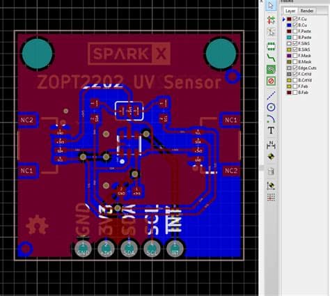
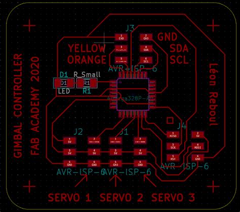
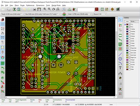
Creating the PCB Layout
Once you have completed the schematic design, you can proceed to create the PCB layout. To do this:
- In the KiCad project tree, right-click on the schematic file and select “Assign PCB Footprints to Schematic Symbols”.
- Assign the appropriate footprints to each component in the schematic.
- Generate the netlist by selecting “Tools” > “Generate Netlist File”.
- Open the PCB Layout Editor by double-clicking on the “PCB Layout Editor” icon in the project tree.
- Import the netlist by selecting “File” > “Import” > “Netlist”.
- Arrange the components on the PCB and route the tracks using the available tools.
- Add any necessary text, graphics, or copper fills to the PCB.
- Perform a design rule check (DRC) to ensure that your PCB meets the manufacturing requirements.
- Generate the Gerber files for manufacturing by selecting “File” > “Plot”.
Advanced KiCad Features
3D Viewer
KiCad includes a 3D viewer that allows you to visualize your PCB design in three dimensions. To use the 3D viewer:
- Open your PCB layout in the PCB Layout Editor.
- Select “View” > “3D Viewer”.
- Use the available navigation tools to rotate, pan, and zoom the 3D view of your PCB.
Scripting and Automation
KiCad supports scripting and automation through the Python programming language. This allows you to automate repetitive tasks, create custom tools, and extend the functionality of KiCad. To use scripting in KiCad:
- Install the KiCad scripting module by selecting “Tools” > “Scripting Console”.
- Write your Python script using the KiCad API.
- Run your script from the Scripting Console or integrate it into your design workflow.
Collaboration and Version Control
KiCad supports collaboration and version control through the use of external tools such as Git. To use version control with KiCad:
- Create a Git repository for your KiCad project.
- Add your KiCad project files to the repository.
- Use Git commands to track changes, create branches, and merge contributions from other team members.
KiCad PCB Design Tutorials and Resources
To help you get started with KiCad and improve your PCB design skills, there are numerous tutorials and resources available online. Some of the best resources include:
- Official KiCad Documentation: https://docs.kicad.org/
- KiCad Forums: https://forum.kicad.info/
- KiCad Tutorials on YouTube: https://www.youtube.com/results?search_query=kicad+tutorial
- KiCad Courses on Udemy: https://www.udemy.com/topic/kicad/
- KiCad Tutorials on Hackster.io: https://www.hackster.io/search?q=kicad
Frequently Asked Questions (FAQ)
1. Is KiCad really free?
Yes, KiCad is completely free and open-source software. You can download, use, and modify KiCad without any cost or licensing fees.
2. Can KiCad be used for commercial projects?
Yes, KiCad can be used for both personal and commercial projects. The open-source license allows you to use KiCad for any purpose, including commercial applications.
3. Is KiCad suitable for beginners?
While KiCad has a learning curve, it is suitable for beginners who are willing to invest time in learning the software. There are numerous tutorials and resources available to help beginners get started with KiCad.
4. Can KiCad import designs from other PCB software?
KiCad can import designs from other PCB software using various file formats, such as Eagle, Altium, and OrCAD. However, the success of the import depends on the compatibility of the file formats and the complexity of the design.
5. Does KiCad support multi-layer PCBs?
Yes, KiCad supports the design of multi-layer PCBs. You can specify the number of layers and their properties in the PCB Layout Editor.
Conclusion
KiCad is a powerful and versatile PCB design software that offers a cost-effective and accessible solution for electronic designers. With its wide range of features, cross-platform compatibility, and active community support, KiCad is an excellent choice for both beginners and experienced designers.
By following the steps outlined in this article, you can download, install, and start using KiCad for your PCB design projects. With the help of tutorials and resources available online, you can quickly learn the basics of KiCad and advance your PCB design skills.
Whether you are a hobbyist working on personal projects or a professional designer creating commercial products, KiCad provides the tools and flexibility you need to bring your electronic designs to life.
No responses yet