Introduction to Keyboard PCB Design
A keyboard PCB (Printed Circuit Board) is the foundation of any custom mechanical keyboard. It is the heart of the keyboard, connecting all the components and allowing for customization. Designing a keyboard PCB requires knowledge of electronics, mechanical design, and software. In this article, we will dive into the world of keyboard PCB design, exploring the factors necessary to build one and the steps involved in the design process.
What is a Keyboard PCB?
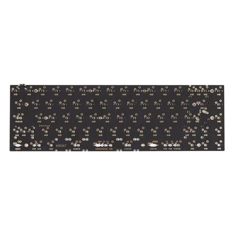
A keyboard PCB is a printed circuit board that houses all the electronic components of a keyboard, including switches, diodes, resistors, and microcontrollers. The PCB acts as a map, guiding the electrical signals from the switches to the microcontroller, which then communicates with the computer.
Components of a Keyboard PCB
-
Switches: The switches are the mechanical components that register key presses. They come in various types, such as Cherry MX, Gateron, and Kailh, each with different characteristics.
-
Diodes: Diodes are used to prevent ghosting, which occurs when multiple keys are pressed simultaneously, causing unintended key presses to register.
-
Resistors: Resistors are used to limit the current flow and protect the components from damage.
-
Microcontroller: The microcontroller is the brain of the keyboard, responsible for processing the key presses and sending the corresponding signals to the computer.
-
USB Connector: The USB connector is used to connect the keyboard to the computer.

Factors to Consider When Designing a Keyboard PCB
1. Keyboard Layout
The first factor to consider when designing a keyboard PCB is the layout. The layout determines the number and arrangement of keys on the keyboard. There are several standard layouts, such as ANSI, ISO, and JIS, each with different key sizes and positions.
| Layout | Description |
|---|---|
| ANSI | The most common layout in the US, with a long Enter key and a single-line Backspace key |
| ISO | The most common layout in Europe, with a short Enter key and a double-line Backspace key |
| JIS | The most common layout in Japan, with a shorter Space bar and additional keys for Japanese characters |
2. Switch Type
The next factor to consider is the type of switches to use. There are several types of switches, each with different characteristics, such as actuation force, travel distance, and tactile feedback.
| Switch Type | Description |
|---|---|
| Linear | Smooth keystroke with no tactile feedback |
| Tactile | Distinct bump at the actuation point |
| Clicky | Tactile bump and audible click at the actuation point |
3. Diode Configuration
The diode configuration determines how the switches are connected to the microcontroller. There are two common configurations: row-to-column and column-to-row.
| Configuration | Description |
|---|---|
| Row-to-Column | Diodes are connected from each switch to the corresponding row pin on the microcontroller |
| Column-to-Row | Diodes are connected from each switch to the corresponding column pin on the microcontroller |
4. Microcontroller Selection
The microcontroller is the brain of the keyboard, responsible for processing the key presses and sending the corresponding signals to the computer. When selecting a microcontroller, consider the following factors:
- Number of I/O pins
- Processing speed
- Memory capacity
- USB connectivity
- Firmware support
Some popular microcontrollers for keyboard PCBs include:
- Atmega32U4
- STM32
- Teensy
5. PCB Thickness and Material
The thickness and material of the PCB can affect its durability and performance. A thicker PCB is more durable and resistant to flexing, while a thinner PCB is lighter and more flexible.
Common PCB materials include:
- FR-4: A glass-reinforced epoxy laminate, commonly used for its high strength and low cost
- Aluminum: A metal PCB that provides better heat dissipation and EMI shielding
6. Mounting Options
The mounting options determine how the PCB is secured inside the keyboard case. There are several mounting options, including:
- Tray mount: The PCB is secured to a tray that sits inside the case
- Top mount: The PCB is secured to the top of the case
- Gasket mount: The PCB is sandwiched between gaskets that provide a soft and flexible typing experience

Keyboard PCB Design Process
1. Schematic Design
The first step in designing a keyboard PCB is to create a schematic diagram. The schematic diagram shows the electrical connections between the components, including the switches, diodes, resistors, and microcontroller.
2. PCB Layout
Once the schematic is complete, the next step is to create the PCB layout. The PCB layout shows the physical arrangement of the components on the board, including the traces that connect them.
When creating the PCB layout, consider the following factors:
- Component placement: Place the components in a logical and efficient manner, minimizing the length of the traces and avoiding interference between components
- Trace width: Use appropriate trace widths for the current requirements of each component
- Via placement: Use vias to connect traces on different layers of the PCB, minimizing the number of vias and placing them in areas that are not prone to stress
- Grounding: Provide adequate grounding for the components to minimize noise and interference
3. Prototyping and Testing
After the PCB layout is complete, the next step is to create a prototype of the PCB. The prototype can be used to test the functionality of the keyboard and identify any issues with the design.
When testing the prototype, consider the following factors:
- Functionality: Test each key to ensure that it registers correctly and that there are no ghosting or rollover issues
- Firmware: Test the firmware to ensure that it is compatible with the microcontroller and that it provides the desired functionality
- Compatibility: Test the keyboard with different operating systems and devices to ensure compatibility
4. Production
Once the prototype has been tested and any issues have been addressed, the final step is to send the PCB design to a manufacturer for production. When selecting a manufacturer, consider the following factors:
- Quality: Choose a manufacturer with a reputation for producing high-quality PCBs
- Lead time: Consider the lead time required for production and ensure that it aligns with your project timeline
- Cost: Compare the costs of different manufacturers to ensure that you are getting the best value for your money

Conclusion
Designing a keyboard PCB requires knowledge of electronics, mechanical design, and software. By considering the factors necessary to build a keyboard PCB and following the design process outlined in this article, you can create a custom keyboard that meets your specific needs and preferences.
Frequently Asked Questions (FAQ)
-
What is the difference between a hot-swappable and soldered PCB?
A hot-swappable PCB allows you to easily remove and replace switches without soldering, while a soldered PCB requires you to solder the switches directly to the board. -
Can I use any type of switch with any PCB?
No, different switches have different pin configurations and may not be compatible with all PCBs. Make sure to choose a PCB that is compatible with your desired switch type. -
What is the difference between a plate-mounted and PCB-mounted stabilizer?
A plate-mounted stabilizer attaches to the switch plate, while a PCB-mounted stabilizer attaches directly to the PCB. PCB-mounted stabilizers provide a more stable typing experience but may be more difficult to install. -
How do I program my keyboard PCB?
Most keyboard PCBs use open-source firmware such as QMK or TMK, which allow you to customize the keyboard layout and functionality using a programming language such as C++. -
Can I design a keyboard PCB without prior experience in electronics?
While it is possible to design a keyboard PCB without prior experience, it is recommended to have a basic understanding of electronics and PCB design principles to ensure a successful project. There are many resources available online to help you learn the basics of PCB design, including tutorials, forums, and open-source projects.
No responses yet