Introduction to PCB Routing
Printed Circuit Board (PCB) routing is a crucial step in the design and manufacturing of electronic devices. It involves the process of connecting various components on a PCB using conductive traces, while adhering to design rules and constraints. Interactive routing PCB refers to the use of specialized software tools that allow designers to manually route the traces on a PCB, as opposed to automated routing where the software determines the optimal path for the traces.
The Importance of PCB Routing
PCB routing plays a significant role in the overall performance and reliability of an electronic device. Properly routed traces ensure that signals are transmitted efficiently between components, minimizing signal integrity issues such as crosstalk, electromagnetic interference (EMI), and signal reflections. Additionally, well-designed PCB routing can help optimize the manufacturing process, reduce costs, and improve the overall quality of the final product.
PCB Routing Techniques
There are several techniques and strategies used in PCB routing to achieve optimal results. Some of the most common techniques include:
Manual Routing
Manual routing involves the designer manually placing and connecting traces between components using a PCB design software. This technique allows for precise control over the routing process and is often used for critical or high-speed signals that require specific routing constraints.
Autorouting
Autorouting is an automated process where the PCB design software determines the optimal path for the traces based on predefined design rules and constraints. This technique is faster than manual routing and is suitable for less critical signals or large, complex designs.
Differential Pair Routing
Differential pair routing is a technique used for high-speed signals that require a balanced transmission line. In this technique, two traces are routed in parallel, with a specific spacing between them, to minimize signal integrity issues and maintain a consistent impedance throughout the signal path.
Length Matching
Length matching is a technique used to ensure that signals arrive at their destination at the same time, minimizing signal skew and improving overall signal integrity. This is achieved by adjusting the length of the traces to match the delay of the slowest signal in the group.
PCB Routing Constraints and Design Rules
To ensure the manufacturability and reliability of a PCB, designers must adhere to various constraints and design rules during the routing process. Some of the most common constraints and design rules include:
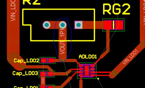
Trace Width and Spacing
Trace width and spacing refer to the minimum width of the conductive traces and the minimum distance between them. These values are determined by the manufacturing capabilities of the PCB fabricator and the electrical requirements of the design.
Via Size and Spacing
Vias are used to connect traces between different layers of a PCB. The size and spacing of the vias must be carefully considered to ensure proper manufacturing and signal integrity.
Copper Pour and Ground Planes
Copper pour and ground planes are used to provide a low-impedance return path for signals and to shield sensitive signals from interference. The design and placement of these features must be carefully considered to optimize their effectiveness.
Clearance and Creepage
Clearance refers to the minimum distance between conductive features on a PCB, while creepage refers to the minimum distance along the surface of the PCB between conductive features. These values are determined by the voltage and environmental requirements of the design.

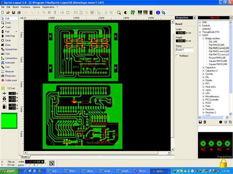
Interactive Routing PCB Software
There are several software tools available for interactive PCB routing, each with its own set of features and capabilities. Some of the most popular interactive routing PCB software include:
| Software | Manufacturer | Key Features |
|---|---|---|
| Altium Designer | Altium | Advanced routing tools, 3D modeling, simulation |
| OrCAD PCB Designer | Cadence | Constraint-driven routing, signal integrity analysis |
| EAGLE PCB | Autodesk | User-friendly interface, extensive component libraries |
| KiCad EDA | Open Source | Free, cross-platform, community-driven development |
These software tools provide designers with a range of features and capabilities to streamline the PCB routing process, including advanced routing algorithms, constraint management, and signal integrity analysis.
Best Practices for Interactive PCB Routing
To achieve optimal results when using interactive routing PCB software, designers should follow these best practices:
- Clearly define design requirements and constraints before starting the routing process.
- Use a consistent naming convention for components, nets, and layers to improve readability and maintainability.
- Route critical or high-speed signals first, using manual routing techniques if necessary.
- Use appropriate trace widths and spacings based on the electrical requirements and manufacturing capabilities.
- Minimize the number of vias and layer changes to improve signal integrity and manufacturability.
- Use copper pour and ground planes to provide a low-impedance return path and shield sensitive signals.
- Perform design rule checks (DRC) and signal integrity analysis regularly to identify and resolve issues early in the design process.
By following these best practices, designers can create high-quality PCB layouts that meet the performance, reliability, and manufacturability requirements of their projects.
Frequently Asked Questions (FAQ)
1. What is the difference between interactive and automated PCB routing?
Interactive PCB routing involves the designer manually placing and connecting traces between components using a PCB design software, while automated routing relies on the software to determine the optimal path for the traces based on predefined design rules and constraints.
2. What are the benefits of using interactive routing PCB software?
Interactive routing PCB software provides designers with precise control over the routing process, allowing them to optimize the layout for critical or high-speed signals. It also enables designers to quickly iterate and make changes to the layout as needed, improving the overall design process.
3. What are some common design rules and constraints in PCB routing?
Common design rules and constraints in PCB routing include trace width and spacing, via size and spacing, copper pour and ground planes, and clearance and creepage. These rules are determined by the manufacturing capabilities of the PCB fabricator and the electrical requirements of the design.
4. How can I ensure signal integrity in my PCB layout?
To ensure signal integrity in your PCB layout, use appropriate trace widths and spacings, minimize the number of vias and layer changes, use copper pour and ground planes to provide a low-impedance return path, and perform regular design rule checks and signal integrity analysis.
5. What are some best practices for interactive PCB routing?
Some best practices for interactive PCB routing include clearly defining design requirements and constraints, using a consistent naming convention, routing critical or high-speed signals first, minimizing the number of vias and layer changes, using copper pour and ground planes, and performing regular design rule checks and signal integrity analysis.
Conclusion
Interactive routing PCB is a powerful technique for creating high-quality PCB layouts that meet the performance, reliability, and manufacturability requirements of modern electronic devices. By using specialized software tools and following best practices, designers can optimize their layouts for critical or high-speed signals, minimize signal integrity issues, and streamline the overall design process.
As the complexity of electronic devices continues to increase, the importance of effective PCB routing will only continue to grow. By staying up-to-date with the latest techniques, tools, and best practices, designers can ensure that their PCB layouts are able to meet the evolving demands of the industry.
No responses yet