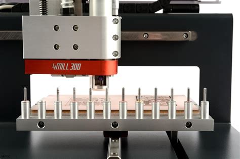
Introduction to PCB Machining
Printed Circuit Board (PCB) machining is an essential process in the manufacturing of electronic devices. It involves creating holes, slots, and other features on the PCB to accommodate various components and connectors. PCB machining includes several techniques such as drilling, milling, routing, and punching. These processes are used to create precise and accurate features on the PCB, ensuring proper functionality and reliability of the electronic device.
Types of PCB Machining
-
Drilling: Drilling is the most common PCB machining process. It involves creating holes in the PCB to accommodate through-hole components and vias. The holes are typically drilled using a computer-controlled drill machine.
-
Milling: Milling is a process used to create slots, pockets, and other features on the PCB. It involves using a rotating cutting tool to remove material from the PCB surface. Milling is often used to create custom shapes and features that cannot be achieved through drilling alone.
-
Routing: Routing is a process used to create the outline of the PCB. It involves using a rotating cutting tool to remove material from the edges of the PCB, creating the desired shape and size.
-
Punching: Punching is a process used to create larger holes and slots in the PCB. It involves using a punch and die set to cut through the PCB material.
Indicating Slots in Your PCB Design
Slots are elongated holes in the PCB that are used to accommodate connectors, switches, and other components. They are typically created using a milling process. When designing a PCB, it is important to indicate the location and size of the slots to ensure proper manufacturing.
Types of Slots
-
Rectangular Slots: Rectangular slots are the most common type of slots used in PCB design. They are used to accommodate connectors and switches that require a rectangular opening in the PCB.
-
Rounded Slots: Rounded slots are used to accommodate components that require a rounded opening in the PCB. They are typically used for connectors and switches with rounded edges.
-
Angled Slots: Angled slots are used to accommodate components that require an angled opening in the PCB. They are typically used for connectors and switches that are mounted at an angle.
Indicating Slots in Your PCB Design Software
Most PCB design software packages include tools for indicating slots in your design. These tools allow you to specify the location, size, and shape of the slots. Here are some tips for indicating slots in your PCB design software:
-
Use the Slot Tool: Most PCB design software packages include a dedicated slot tool that allows you to create slots with just a few clicks. Simply select the slot tool, specify the location and size of the slot, and the software will create it for you.
-
Specify the Slot Dimensions: When creating a slot, it is important to specify the exact dimensions of the slot. This includes the length, width, and depth of the slot. Make sure to double-check these dimensions to ensure that they match the requirements of the component that will be mounted in the slot.
-
Use the Correct Layer: When creating a slot, make sure to place it on the correct layer in your PCB design software. Most slots should be placed on the top or bottom layer of the PCB, depending on where the component will be mounted.
Best Practices for Indicating Slots
-
Keep Slots Away from Board Edges: When placing slots in your PCB design, it is important to keep them away from the edges of the board. This helps to prevent damage to the slots during the manufacturing process and ensures that the components mounted in the slots will be secure.
-
Use Standard Slot Sizes: Whenever possible, use standard slot sizes in your PCB design. This helps to ensure compatibility with standard components and reduces the cost and complexity of the manufacturing process.
-
Provide Adequate Clearance: When placing slots in your PCB design, make sure to provide adequate clearance around the slots for the components that will be mounted in them. This helps to ensure proper fit and function of the components.

Indicating Milling in Your PCB Design
Milling is a process used to create custom shapes and features on the PCB surface. It involves using a rotating cutting tool to remove material from the PCB. When designing a PCB, it is important to indicate the location and size of the milled features to ensure proper manufacturing.
Types of Milled Features
-
Pockets: Pockets are shallow recesses milled into the surface of the PCB. They are typically used to accommodate components that require a flush mount with the PCB surface.
-
Cavities: Cavities are deeper recesses milled into the surface of the PCB. They are typically used to accommodate larger components or to provide additional clearance between the component and the PCB surface.
-
Channels: Channels are long, narrow recesses milled into the surface of the PCB. They are typically used to route wires or to provide additional clearance between components.
Indicating Milling in Your PCB Design Software
Most PCB design software packages include tools for indicating milled features in your design. These tools allow you to specify the location, size, and shape of the milled features. Here are some tips for indicating milling in your PCB design software:
-
Use the Mill Tool: Most PCB design software packages include a dedicated mill tool that allows you to create milled features with just a few clicks. Simply select the mill tool, specify the location and size of the feature, and the software will create it for you.
-
Specify the Milling Depth: When creating a milled feature, it is important to specify the depth of the milling. This is typically measured from the surface of the PCB to the bottom of the milled feature. Make sure to double-check this dimension to ensure that it matches the requirements of the component that will be mounted in the feature.
-
Use the Correct Layer: When creating a milled feature, make sure to place it on the correct layer in your PCB design software. Most milled features should be placed on the top or bottom layer of the PCB, depending on where the component will be mounted.
Best Practices for Indicating Milling
-
Keep Milled Features Away from Board Edges: When placing milled features in your PCB design, it is important to keep them away from the edges of the board. This helps to prevent damage to the features during the manufacturing process and ensures that the components mounted in the features will be secure.
-
Use Standard Milling Depths: Whenever possible, use standard milling depths in your PCB design. This helps to ensure compatibility with standard components and reduces the cost and complexity of the manufacturing process.
-
Provide Adequate Clearance: When placing milled features in your PCB design, make sure to provide adequate clearance around the features for the components that will be mounted in them. This helps to ensure proper fit and function of the components.

Indicating Contour in Your PCB Design
Contour is the process of creating the outline of the PCB. It involves using a rotating cutting tool to remove material from the edges of the PCB, creating the desired shape and size. When designing a PCB, it is important to indicate the contour of the board to ensure proper manufacturing.
Types of Contours
-
Standard Contours: Standard contours are the most common type of contours used in PCB design. They include simple shapes such as rectangles, circles, and ovals.
-
Custom Contours: Custom contours are used to create unique shapes and sizes for the PCB. They can include complex curves, angles, and other features that are not possible with standard contours.
Indicating Contour in Your PCB Design Software
Most PCB design software packages include tools for indicating contour in your design. These tools allow you to specify the shape and size of the PCB outline. Here are some tips for indicating contour in your PCB design software:
-
Use the Contour Tool: Most PCB design software packages include a dedicated contour tool that allows you to create the PCB outline with just a few clicks. Simply select the contour tool, specify the shape and size of the PCB, and the software will create it for you.
-
Specify the Contour Dimensions: When creating a contour, it is important to specify the exact dimensions of the PCB. This includes the length, width, and any other relevant dimensions. Make sure to double-check these dimensions to ensure that they match the requirements of the device that the PCB will be used in.
-
Use the Correct Layer: When creating a contour, make sure to place it on the correct layer in your PCB design software. Most contours should be placed on the outline layer of the PCB.
Best Practices for Indicating Contour
-
Keep Contours Simple: When designing the contour of your PCB, it is important to keep it as simple as possible. Complex contours can be more difficult and expensive to manufacture, and may not provide any significant benefit to the functionality of the device.
-
Use Standard Sizes: Whenever possible, use standard sizes for your PCB contour. This helps to reduce the cost and complexity of the manufacturing process, and ensures compatibility with standard enclosures and other components.
-
Provide Adequate Clearance: When designing the contour of your PCB, make sure to provide adequate clearance around the edges of the board for the components and other features that will be mounted on it. This helps to ensure proper fit and function of the device.

Indicating Rout-outs in Your PCB Design
Rout-outs are areas of the PCB that are removed to create openings for components, connectors, or other features. They are typically created using a routing process, which involves using a rotating cutting tool to remove material from the PCB. When designing a PCB, it is important to indicate the location and size of the rout-outs to ensure proper manufacturing.
Types of Rout-outs
-
Component Rout-outs: Component rout-outs are used to create openings in the PCB for components that require a specific mounting arrangement. They are typically used for larger components such as transformers, heat sinks, and connectors.
-
Connector Rout-outs: Connector rout-outs are used to create openings in the PCB for connectors that require a specific mounting arrangement. They are typically used for larger connectors such as power connectors and high-density connectors.
-
Mounting Rout-outs: Mounting rout-outs are used to create openings in the PCB for mounting hardware such as screws, standoffs, and brackets. They are typically used to provide additional support and stability for the PCB and its components.
Indicating Rout-outs in Your PCB Design Software
Most PCB design software packages include tools for indicating rout-outs in your design. These tools allow you to specify the location, size, and shape of the rout-outs. Here are some tips for indicating rout-outs in your PCB design software:
-
Use the Rout-out Tool: Most PCB design software packages include a dedicated rout-out tool that allows you to create rout-outs with just a few clicks. Simply select the rout-out tool, specify the location and size of the rout-out, and the software will create it for you.
-
Specify the Rout-out Dimensions: When creating a rout-out, it is important to specify the exact dimensions of the opening. This includes the length, width, and depth of the rout-out. Make sure to double-check these dimensions to ensure that they match the requirements of the component or connector that will be mounted in the rout-out.
-
Use the Correct Layer: When creating a rout-out, make sure to place it on the correct layer in your PCB design software. Most rout-outs should be placed on the top or bottom layer of the PCB, depending on where the component or connector will be mounted.
Best Practices for Indicating Rout-outs
-
Keep Rout-outs Away from Board Edges: When placing rout-outs in your PCB design, it is important to keep them away from the edges of the board. This helps to prevent damage to the rout-outs during the manufacturing process and ensures that the components and connectors mounted in the rout-outs will be secure.
-
Use Standard Rout-out Sizes: Whenever possible, use standard rout-out sizes in your PCB design. This helps to ensure compatibility with standard components and connectors, and reduces the cost and complexity of the manufacturing process.
-
Provide Adequate Clearance: When placing rout-outs in your PCB design, make sure to provide adequate clearance around the rout-outs for the components and connectors that will be mounted in them. This helps to ensure proper fit and function of the components and connectors.
Table: PCB Machining Techniques and Their Uses
| Machining Technique | Description | Uses |
|---|---|---|
| Drilling | Creating holes in the PCB to accommodate through-hole components and vias | Mounting through-hole components, creating vias for interlayer connections |
| Milling | Creating slots, pockets, and other features on the PCB surface | Accommodating components that require a flush mount or additional clearance |
| Routing | Creating the outline of the PCB | Defining the shape and size of the PCB |
| Punching | Creating larger holes and slots in the PCB | Accommodating larger components and connectors |
Frequently Asked Questions (FAQs)
- What is the difference between drilling and milling in PCB machining?
-
Drilling is used to create holes in the PCB for through-hole components and vias, while milling is used to create slots, pockets, and other features on the PCB surface.
-
Can I use any shape for my PCB contour?
-
While custom contours are possible, it is generally best to use standard shapes such as rectangles, circles, and ovals for your PCB contour to reduce manufacturing complexity and cost.
-
How do I ensure proper clearance for components mounted in slots and rout-outs?
-
When designing slots and rout-outs, make sure to provide adequate clearance around them for the components that will be mounted in them. This helps to ensure proper fit and function of the components.
-
What is the purpose of indicating machining features in my PCB design software?
-
Indicating machining features such as slots, milling, contour, and rout-outs in your PCB design software helps to ensure that the PCB is manufactured correctly and that all components and connectors fit and function properly.
-
Can I use non-standard sizes for slots and rout-outs in my PCB design?
- While non-standard sizes are possible, it is generally best to use standard sizes for slots and rout-outs in your PCB design to reduce manufacturing complexity and cost, and to ensure compatibility with standard components and connectors.
Conclusion
PCB machining is a critical process in the manufacturing of electronic devices. It involves creating holes, slots, and other features on the PCB to accommodate various components and connectors. When designing a PCB, it is important to indicate the location and size of these features to ensure proper manufacturing.
By following best practices for indicating slots, milling, contour, and rout-outs in your PCB design software, you can help to ensure that your PCB is manufactured correctly and that all components and connectors fit and function properly. This includes using standard sizes and shapes whenever possible, providing adequate clearance for components, and keeping machined features away from board edges.
By working closely with your PCB Manufacturer and providing clear and accurate design files, you can help to streamline the manufacturing process and ensure the highest quality and reliability for your electronic devices.
No responses yet