Introduction to PCB Design
Printed Circuit Board (PCB) design is a crucial aspect of modern electronics manufacturing. PCBs are the backbone of almost every electronic device, from smartphones and computers to industrial equipment and medical devices. The quality of a PCB directly affects the performance, reliability, and longevity of the final product. In this comprehensive guide, we will delve into the intricacies of PCB design, including design details, best practices, and common challenges faced by designers.
The Importance of PCB Design
PCB design plays a vital role in the success of an electronic product. A well-designed PCB ensures that the electronic components are properly connected, signals are routed efficiently, and the board can withstand the rigors of its intended operating environment. Poor PCB design can lead to a range of issues, such as signal integrity problems, electromagnetic interference (EMI), thermal management challenges, and manufacturability difficulties.
The Impact of PCB Design on Product Performance
The performance of an electronic product is directly linked to the quality of its PCB design. Factors such as signal integrity, power distribution, and component placement all contribute to the overall performance of the device. For example, improper signal routing can lead to crosstalk, reflections, and other signal integrity issues that can degrade the performance of high-speed digital circuits. Similarly, poor power distribution can result in voltage drops, noise, and other power-related problems that can affect the stability and reliability of the product.
PCB Design and Manufacturability
PCB design also has a significant impact on the manufacturability of the board. A design that is difficult or impossible to manufacture can lead to production delays, increased costs, and reduced product quality. Designers must consider factors such as component placement, trace widths and spacings, via sizes, and soldermask and silkscreen requirements to ensure that the board can be efficiently and reliably manufactured.

The PCB Design Process
The PCB design process typically involves several key stages, each with its own set of challenges and considerations. These stages include:
- Schematic capture
- Component selection and placement
- PCB layout and routing
- Design rule checking (DRC) and verification
- Generating manufacturing files
Schematic Capture
Schematic capture is the first step in the PCB design process. It involves creating a graphical representation of the electronic circuit, showing the interconnections between components. The schematic serves as a blueprint for the PCB layout and is used to verify the logical correctness of the circuit.
When creating a schematic, designers must consider factors such as:
- Component selection and compatibility
- Power supply requirements
- Signal integrity and noise reduction techniques
- Testability and debugging features
Component Selection and Placement
Once the schematic is complete, the next step is to select and place the components on the PCB. Component selection involves choosing the appropriate components based on factors such as performance requirements, cost, availability, and reliability. Component placement is the process of arranging the components on the board in a way that optimizes signal routing, thermal management, and manufacturability.
When placing components, designers must consider:
- Component footprints and land patterns
- Placement density and board size constraints
- Signal integrity and crosstalk reduction
- Thermal management and heat dissipation
- Manufacturing constraints, such as pick-and-place machine capabilities
PCB Layout and Routing
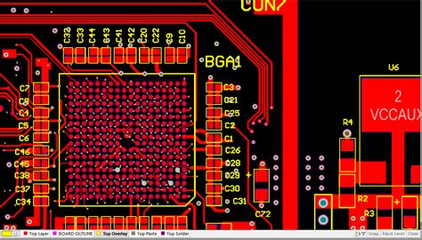
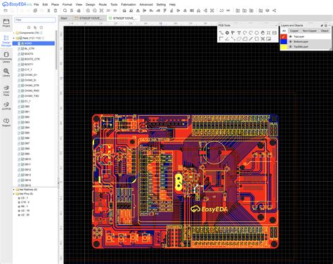
PCB layout and routing is the process of creating the physical design of the PCB, including the placement of components, the routing of traces, and the creation of power and ground planes. The goal of PCB layout is to create a design that meets the electrical, mechanical, and thermal requirements of the circuit while also being manufacturable and cost-effective.
When laying out a PCB, designers must consider:
- Board stack-up and layer arrangement
- Trace widths and spacings
- Via sizes and placement
- Power and ground plane design
- High-speed signal routing techniques
- Electromagnetic compatibility (EMC) and EMI reduction
Design Rule Checking (DRC) and Verification
Design rule checking (DRC) is the process of verifying that the PCB layout meets the design rules specified by the manufacturer and the designer. DRC helps to identify potential issues such as shorts, opens, and violations of trace width and spacing requirements. Verification is the process of ensuring that the PCB layout matches the schematic and meets the functional requirements of the circuit.
When performing DRC and verification, designers must consider:
- Manufacturing constraints and capabilities
- Electrical rules, such as trace widths and spacings
- Signal integrity and timing requirements
- Thermal and mechanical constraints
- Regulatory requirements, such as safety and EMC standards
Generating Manufacturing Files
The final step in the PCB design process is generating the manufacturing files that will be used to fabricate and assemble the board. These files typically include:
- Gerber files for each layer of the PCB
- Drill files for specifying hole locations and sizes
- Bill of Materials (BOM) for component procurement
- Assembly drawings and instructions
When generating manufacturing files, designers must ensure that the files are accurate, complete, and comply with the manufacturer’s specifications.

PCB Design Best Practices
To create high-quality PCBs that meet the required performance, reliability, and manufacturability criteria, designers should follow a set of best practices. Some of these best practices include:
Designing for Manufacturability (DFM)
Designing for manufacturability (DFM) involves creating a PCB design that is optimized for the manufacturing process. This includes considering factors such as:
- Component placement and orientation
- Trace widths and spacings
- Via sizes and placement
- Soldermask and silkscreen requirements
- Panelization and break-away tabs
By designing with manufacturability in mind, designers can reduce production costs, improve yield rates, and ensure a more reliable end product.
Signal Integrity and Power Integrity
Maintaining signal integrity and power integrity is crucial for ensuring the proper functioning of the electronic circuit. Signal integrity refers to the quality of the signals transmitted through the PCB, while power integrity relates to the quality of the power distribution network.
To maintain signal and power integrity, designers should:
- Use appropriate trace widths and spacings
- Implement proper termination and impedance matching techniques
- Use ground planes and power planes to reduce noise and improve power distribution
- Minimize crosstalk and electromagnetic interference (EMI)
- Consider the effects of vias and connectors on signal quality
Thermal Management
Thermal management is the process of ensuring that the PCB and its components can operate within their specified temperature ranges. Overheating can lead to reduced performance, reliability issues, and even device failure.
To manage thermal issues, designers should:
- Select components with appropriate power ratings and thermal characteristics
- Use thermal management techniques such as heatsinks, thermal vias, and copper pours
- Consider the effects of component placement and orientation on heat dissipation
- Use thermal simulation tools to predict and optimize the thermal performance of the PCB
Documentation and Version Control
Proper documentation and version control are essential for ensuring the accuracy, consistency, and traceability of the PCB design. Designers should maintain a complete set of design files, including schematics, layouts, and manufacturing files, and use version control systems to track changes and collaborate with other team members.

Common PCB Design Challenges and Solutions
PCB designers often face a variety of challenges when creating high-quality boards. Some of the most common challenges and their solutions include:
Controlling Electromagnetic Interference (EMI)
EMI can cause signal integrity issues and may lead to non-compliance with regulatory standards. To reduce EMI, designers can:
- Use proper grounding and shielding techniques
- Minimize loop areas and use differential signaling
- Separate high-speed signals from low-speed signals
- Use filters and suppression components
Managing High-Speed Signals
High-speed signals, such as those found in high-frequency digital circuits, require special consideration in PCB design. To manage high-speed signals, designers should:
- Use controlled impedance traces and termination techniques
- Minimize trace lengths and use length matching
- Implement proper signal return paths
- Use simulation tools to analyze and optimize signal integrity
Dealing with Limited Board Space
As electronic devices become smaller and more complex, PCB designers often face the challenge of fitting all the necessary components and traces into a limited board space. To overcome this challenge, designers can:
- Use smaller component packages, such as chip-scale packages (CSPs) and ball grid arrays (BGAs)
- Implement high-density interconnect (HDI) techniques, such as microvias and blind/buried vias
- Use multi-layer PCBs to increase routing density
- Optimize component placement and orientation
Ensuring Manufacturability
Ensuring that a PCB design is manufacturable is critical for avoiding production delays and reducing costs. To improve manufacturability, designers should:
- Follow the manufacturer’s design rules and guidelines
- Use standard component footprints and land patterns
- Minimize the use of non-standard hole sizes and shapes
- Incorporate design for manufacturability (DFM) techniques, such as avoiding acute angles and using appropriate trace widths and spacings
Conclusion
PCB design is a complex and multi-faceted process that requires a deep understanding of electronic circuits, manufacturing processes, and design best practices. By following the guidelines and techniques outlined in this article, designers can create high-quality PCBs that meet the performance, reliability, and manufacturability requirements of modern electronic devices.
Frequently Asked Questions (FAQ)
-
What is the difference between a schematic and a PCB layout?
A schematic is a graphical representation of an electronic circuit, showing the interconnections between components. A PCB layout, on the other hand, is the physical design of the printed circuit board, including the placement of components, routing of traces, and creation of power and ground planes. -
What are vias, and why are they used in PCB design?
Vias are small holes drilled through a PCB that allow signals to pass from one layer of the board to another. They are used to create electrical connections between layers and to route signals in multi-layer PCBs. -
What is the purpose of a ground plane in a PCB?
A ground plane is a large area of copper on one or more layers of a PCB that is connected to the ground potential. Its purpose is to provide a low-impedance return path for signals, reduce noise and EMI, and improve the overall signal integrity of the board. -
What is the difference between a blind via and a buried via?
A blind via is a via that connects an outer layer of a PCB to an inner layer, but does not go through the entire board. A buried via, on the other hand, connects two or more inner layers of a PCB, but does not extend to either of the outer layers. -
What is design for manufacturability (DFM), and why is it important in PCB design?
Design for manufacturability (DFM) is the practice of designing a PCB in a way that optimizes its manufacturability. This involves considering factors such as component placement, trace widths and spacings, via sizes, and soldermask and silkscreen requirements. DFM is important because it helps to reduce production costs, improve yield rates, and ensure a more reliable end product.
| PCB Design Stage | Key Considerations |
|---|---|
| Schematic Capture | – Component selection and compatibility – Power supply requirements – Signal integrity and noise reduction techniques – Testability and debugging features |
| Component Selection and Placement | – Component footprints and land patterns – Placement density and board size constraints – Signal integrity and crosstalk reduction – Thermal management and heat dissipation – Manufacturing constraints |
| PCB Layout and Routing | – Board stack-up and layer arrangement – Trace widths and spacings – Via sizes and placement – Power and ground plane design – High-speed signal routing techniques – Electromagnetic compatibility (EMC) and EMI reduction |
| Design Rule Checking (DRC) and Verification | – Manufacturing constraints and capabilities – Electrical rules, such as trace widths and spacings – Signal integrity and timing requirements – Thermal and mechanical constraints – Regulatory requirements, such as safety and EMC standards |
| Generating Manufacturing Files | – Gerber files for each layer of the PCB – Drill files for specifying hole locations and sizes – Bill of Materials (BOM) for component procurement – Assembly drawings and instructions |

No responses yet