Introduction to IC Substrates
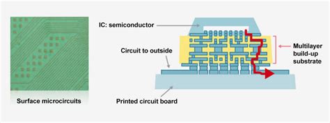
An Integrated Circuit (IC) substrate is a thin, flat material that serves as the foundation for the construction of an IC package. It provides mechanical support, electrical interconnections, and heat dissipation for the IC chip. The substrate is a crucial component in the packaging process, as it directly affects the performance, reliability, and cost of the final IC product.
What is an IC Substrate?
An IC substrate is a thin, flat material that is used as a base for the assembly of an integrated circuit package. It is typically made of a dielectric material, such as ceramic, glass, or organic materials like FR-4 or BT (Bismaleimide Triazine). The substrate has conductive traces and vias that provide electrical connections between the IC chip and the external circuitry.
Functions of an IC Substrate
The primary functions of an IC substrate are:
- Mechanical support: The substrate provides a stable platform for the IC chip and other components to be mounted on.
- Electrical interconnections: The conductive traces and vias on the substrate facilitate electrical connections between the IC chip and the external circuitry.
- Heat dissipation: The substrate helps dissipate heat generated by the IC chip during operation, preventing thermal damage and ensuring optimal performance.
Types of IC Substrates
There are several types of IC substrates, each with its own characteristics and applications. The choice of substrate depends on factors such as the IC package type, performance requirements, and cost considerations.
Ceramic Substrates
Ceramic substrates are made of inorganic materials, such as alumina (Al2O3) or aluminum nitride (AlN). They offer excellent thermal conductivity, high mechanical strength, and good electrical insulation properties. Ceramic substrates are commonly used in high-performance applications, such as power electronics and microwave devices.
Organic Substrates
Organic substrates are made of polymer-based materials, such as FR-4 (Flame Retardant 4) or BT (Bismaleimide Triazine). They are less expensive and easier to manufacture compared to ceramic substrates. Organic substrates are widely used in consumer electronics, such as smartphones, laptops, and gaming consoles.
FR-4 Substrates
FR-4 is a glass-reinforced epoxy laminate material. It is the most common type of organic substrate due to its low cost, good mechanical strength, and acceptable electrical properties. FR-4 substrates are used in a wide range of applications, from low-cost consumer electronics to high-density interconnect (HDI) packages.
BT Substrates
BT substrates are made of a thermosetting polymer called Bismaleimide Triazine. They offer better thermal stability and lower moisture absorption compared to FR-4 substrates. BT substrates are often used in advanced packaging technologies, such as flip-chip ball grid array (FCBGA) and chip-scale packages (CSP).
Glass Substrates
Glass substrates are emerging as a promising alternative to traditional ceramic and organic substrates. They offer several advantages, such as high electrical insulation, low dielectric constant, and excellent dimensional stability. Glass substrates are particularly suitable for high-frequency applications, such as 5G communications and millimeter-wave devices.
Manufacturing Process of IC Substrates
The manufacturing process of IC substrates involves several steps, depending on the type of substrate and the required features. The general process flow for organic substrates is as follows:
- Core layer preparation: The core layer, typically made of FR-4 or BT material, is cut to the desired size and shape.
- Drilling: Holes are drilled through the core layer to create vias for electrical connections between layers.
- Plating: The drilled holes are plated with a conductive material, such as copper, to form the via connections.
- Patterning: The outer layers of the substrate are patterned with conductive traces using photolithography and etching processes.
- Lamination: Additional layers, such as prepreg (pre-impregnated) and copper foils, are laminated onto the core layer to form a multi-layer substrate.
- Surface finishing: The outer layers of the substrate are finished with a protective coating, such as solder mask, and surface treatments, like ENIG (Electroless Nickel Immersion Gold) or OSP (Organic Solderability Preservative), to enhance solderability and prevent oxidation.
For ceramic substrates, the manufacturing process involves steps such as tape casting, punching, screen printing, and firing at high temperatures to create a dense, multi-layer structure.

Key Parameters of IC Substrates
When selecting an IC substrate for a specific application, several key parameters need to be considered:
Dielectric Constant (Dk)
The dielectric constant is a measure of a material’s ability to store electrical energy. A lower Dk value is desirable for high-frequency applications, as it reduces signal Propagation Delay and minimizes cross-talk between adjacent traces.
Dissipation Factor (Df)
The dissipation factor, also known as loss tangent, represents the energy loss in a dielectric material. A lower Df value indicates lower energy loss and is preferred for high-frequency applications.
Thermal Conductivity
Thermal conductivity is a measure of a material’s ability to conduct heat. A higher thermal conductivity is desirable for effective heat dissipation, especially in high-power applications.
Coefficient of Thermal Expansion (CTE)
The CTE indicates how much a material expands or contracts with changes in temperature. A close match between the CTE of the substrate and the IC chip is essential to minimize thermal stress and prevent reliability issues.
Dimensional Stability
Dimensional stability refers to a material’s ability to maintain its size and shape under various environmental conditions, such as temperature and humidity changes. Good dimensional stability is crucial for maintaining the integrity of the electrical connections and preventing warpage.
Advanced Packaging Technologies and IC Substrates
The demand for higher performance, smaller form factors, and increased functionality in electronic devices has driven the development of advanced packaging technologies. These technologies rely heavily on innovative IC substrate solutions to enable their implementation.
2.5D and 3D Packaging
2.5D and 3D packaging technologies involve the vertical stacking of multiple IC chips on a single substrate or the integration of multiple chips on an interposer. These approaches require substrates with high-density interconnects, fine-pitch vias, and excellent thermal management capabilities.
Fan-Out Wafer-Level Packaging (FOWLP)
FOWLP is a packaging technology that involves embedding the IC chip in a molded wafer-like structure and redistributing the connections to a larger area. This approach enables smaller package sizes and improved electrical performance. FOWLP substrates require materials with low warpage, high dimensional stability, and good adhesion properties.
Embedded Die Packaging
Embedded die packaging involves the integration of IC chips within the substrate itself, rather than mounting them on the surface. This technology offers several benefits, such as reduced package thickness, improved electrical performance, and better thermal management. Embedded die packaging requires substrates with precise cavity formation, good dielectric properties, and compatibility with the embedded die materials.
Future Trends in IC Substrates
As the electronics industry continues to evolve, IC substrates must keep pace with the increasing demands for performance, reliability, and cost-effectiveness. Some of the future trends in IC substrates include:
- Adoption of high-frequency materials: With the proliferation of 5G and millimeter-wave applications, there is a growing need for substrates with low dielectric constant and loss tangent, such as glass and advanced ceramic materials.
- Miniaturization and high-density interconnects: The trend towards smaller, more compact electronic devices requires substrates with finer feature sizes, higher via densities, and thinner profiles.
- Integration of passive components: The integration of passive components, such as capacitors and resistors, into the substrate can help reduce package size, improve electrical performance, and simplify the assembly process.
- Sustainable and eco-friendly materials: There is an increasing focus on the development of environmentally friendly substrate materials and processes, such as halogen-free flame retardants and lead-free soldering.
Frequently Asked Questions (FAQ)
1. What is the difference between a ceramic and an organic IC substrate?
Ceramic substrates are made of inorganic materials, such as alumina or aluminum nitride, and offer excellent thermal conductivity, high mechanical strength, and good electrical insulation properties. Organic substrates, on the other hand, are made of polymer-based materials, such as FR-4 or BT, and are less expensive and easier to manufacture compared to ceramic substrates.
2. What is the purpose of vias in an IC substrate?
Vias are conductive paths that facilitate electrical connections between different layers of an IC substrate. They allow signals and power to be routed vertically through the substrate, enabling the creation of complex, multi-layer interconnect structures.
3. Why is the coefficient of thermal expansion (CTE) an important parameter for IC substrates?
The CTE indicates how much a material expands or contracts with changes in temperature. A close match between the CTE of the substrate and the IC chip is essential to minimize thermal stress and prevent reliability issues, such as delamination or cracking.
4. What are the advantages of using glass substrates for high-frequency applications?
Glass substrates offer several advantages for high-frequency applications, such as low dielectric constant, low loss tangent, and excellent dimensional stability. These properties help reduce signal propagation delay, minimize cross-talk between adjacent traces, and maintain the integrity of the electrical connections over a wide range of operating conditions.
5. How do advanced packaging technologies, such as 2.5D and 3D packaging, benefit from innovative IC substrate solutions?
Advanced packaging technologies, like 2.5D and 3D packaging, require substrates with high-density interconnects, fine-pitch vias, and excellent thermal management capabilities. Innovative IC substrate solutions, such as interposers and embedded die substrates, enable the implementation of these technologies by providing the necessary electrical, mechanical, and thermal properties to support the vertical stacking and integration of multiple IC chips.
Conclusion
IC substrates play a crucial role in the packaging and performance of integrated circuits. With the increasing demand for higher performance, smaller form factors, and enhanced functionality in electronic devices, the development of advanced IC substrate solutions has become more important than ever.
From traditional ceramic and organic substrates to emerging materials like glass, IC substrates continue to evolve to meet the challenges of the rapidly advancing electronics industry. By understanding the types, manufacturing processes, key parameters, and future trends in IC substrates, engineers and designers can make informed decisions when selecting the most suitable substrate for their specific applications.
As the electronics landscape continues to change, innovative IC substrate solutions will remain at the forefront of enabling the next generation of high-performance, reliable, and cost-effective electronic devices.
| IC Substrate Type | Advantages | Disadvantages | Common Applications |
|---|---|---|---|
| Ceramic | – High thermal conductivity – High mechanical strength – Good electrical insulation |
– High cost – Difficult to manufacture – Limited design flexibility |
– Power electronics – Microwave devices – High-reliability applications |
| Organic (FR-4) | – Low cost – Good mechanical strength – Acceptable electrical properties |
– Lower thermal conductivity than ceramic – Higher moisture absorption |
– Consumer electronics – High-density interconnect (HDI) packages |
| Organic (BT) | – Better thermal stability than FR-4 – Lower moisture absorption than FR-4 |
– Higher cost than FR-4 – Lower thermal conductivity than ceramic |
– Advanced packaging (FCBGA, CSP) – High-performance applications |
| Glass | – High electrical insulation – Low dielectric constant – Excellent dimensional stability |
– Brittle – Limited thermal conductivity |
– High-frequency applications (5G, mmWave) – Advanced packaging technologies |
No responses yet