Introduction to IC Packaging
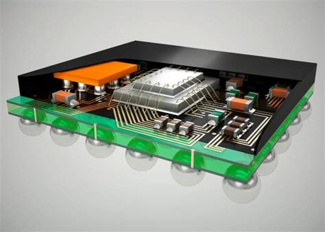
Integrated Circuit (IC) packaging is a crucial aspect of modern electronic devices. It is the process of encasing a semiconductor chip in a protective shell, which provides mechanical support, electrical connectivity, and thermal dissipation. The packaging also serves as an interface between the chip and the outside world, allowing it to be connected to other components on a printed circuit board (PCB).
The Importance of IC Packaging
IC packaging plays a vital role in the performance, reliability, and cost of electronic devices. Some of the key reasons why IC packaging is important include:
-
Protection: The packaging protects the delicate semiconductor chip from physical damage, moisture, and other environmental factors that can affect its performance and reliability.
-
Electrical Connectivity: The packaging provides electrical connections between the chip and the outside world, allowing it to communicate with other components on the PCB.
-
Thermal Management: The packaging helps to dissipate heat generated by the chip, which is essential for maintaining its performance and reliability.
-
Cost: The choice of packaging can have a significant impact on the overall cost of the device, as it affects the manufacturing process, materials used, and testing requirements.
Types of IC Packaging
There are several types of IC packaging available, each with its own advantages and disadvantages. Some of the most common types of IC packaging include:
Through-Hole Packaging
Through-hole packaging is one of the oldest and most reliable types of IC packaging. It involves inserting the leads of the chip through holes in the PCB and soldering them in place. This type of packaging is known for its high mechanical strength and reliability, but it is also relatively large and expensive compared to other types of packaging.
Surface Mount Packaging
Surface mount packaging is a more modern type of IC packaging that has largely replaced through-hole packaging in many applications. It involves soldering the leads of the chip directly onto the surface of the PCB, which allows for smaller and more compact designs. Surface mount packaging is also faster and cheaper to manufacture than through-hole packaging.
Ball Grid Array (BGA) Packaging
Ball Grid Array (BGA) packaging is a type of surface mount packaging that uses an array of solder balls to connect the chip to the PCB. This allows for a higher density of connections than traditional surface mount packaging, which is essential for high-performance devices such as graphics cards and processors. BGA packaging is also more reliable than other types of surface mount packaging, as the solder balls provide a stronger mechanical connection.
Flip Chip Packaging
Flip chip packaging is a type of packaging where the chip is flipped over and connected directly to the PCB using solder bumps. This allows for a very high density of connections and a very small package size, which is essential for applications such as mobile devices and wearables. Flip chip packaging is also very reliable, as the solder bumps provide a strong mechanical connection and good thermal dissipation.

Factors to Consider When Choosing IC Packaging
When choosing an IC packaging for your electronic device, there are several factors to consider. Some of the most important factors include:
Size and Form Factor
The size and form factor of the packaging are important considerations, especially for devices with limited space such as mobile phones and wearables. Smaller packages allow for more compact designs, but they may also have limitations in terms of performance and reliability.
Electrical Performance
The electrical performance of the packaging is another important consideration, especially for high-speed and high-frequency devices. The packaging must provide good signal integrity and low inductance to ensure reliable operation.
Thermal Performance
The thermal performance of the packaging is essential for maintaining the performance and reliability of the device. The packaging must be able to dissipate heat effectively to prevent the chip from overheating and failing.
Cost
The cost of the packaging is also an important consideration, especially for high-volume production. The choice of materials, manufacturing process, and testing requirements can all affect the overall cost of the packaging.

IC Packaging Materials
The materials used in IC packaging play a crucial role in its performance and reliability. Some of the most common materials used in IC packaging include:
Ceramic
Ceramic is a popular material for IC packaging due to its excellent thermal and mechanical properties. It is also resistant to moisture and other environmental factors, making it ideal for high-reliability applications such as aerospace and defense.
Plastic
Plastic is another common material used in IC packaging, especially for consumer electronics. It is cheaper and lighter than ceramic, but it may not provide the same level of thermal and mechanical performance.
Metal
Metal is sometimes used in IC packaging for its excellent thermal and mechanical properties. It is also used for shielding against electromagnetic interference (EMI) in high-frequency applications.

IC Packaging Manufacturing Process
The manufacturing process for IC packaging involves several steps, including:
Die Attachment
The first step in the manufacturing process is to attach the semiconductor die to the substrate or lead frame. This is typically done using an adhesive or solder.
Wire Bonding
The next step is to connect the die to the substrate or lead frame using thin wires. This is typically done using a process called wire bonding, which involves attaching the wires to the bond pads on the die and the substrate or lead frame.
Encapsulation
After the die is attached and connected, it is encapsulated in a protective material such as plastic or ceramic. This provides mechanical support and protection from the environment.
Testing
The final step in the manufacturing process is testing. The packaged device is tested for functionality, reliability, and performance to ensure that it meets the required specifications.
Future Trends in IC Packaging
As electronic devices continue to become smaller, faster, and more complex, the demand for advanced IC packaging solutions will continue to grow. Some of the future trends in IC packaging include:
3D Packaging
3D packaging involves stacking multiple chips on top of each other to create a more compact and high-performance package. This allows for higher density and better thermal management than traditional 2D packaging.
Wafer-Level Packaging
Wafer-level packaging involves packaging the entire wafer before it is diced into individual chips. This allows for smaller package sizes and lower costs than traditional packaging methods.
System-in-Package (SiP)
System-in-Package (SiP) involves integrating multiple chips and components into a single package. This allows for more compact and high-performance devices, especially in applications such as mobile phones and wearables.
FAQ
What is the difference between through-hole and surface mount packaging?
Through-hole packaging involves inserting the leads of the chip through holes in the PCB and soldering them in place, while surface mount packaging involves soldering the leads directly onto the surface of the PCB. Surface mount packaging allows for smaller and more compact designs, while through-hole packaging is known for its high mechanical strength and reliability.
What is the purpose of IC packaging?
The purpose of IC packaging is to provide mechanical support, electrical connectivity, and thermal dissipation for the semiconductor chip. It also serves as an interface between the chip and the outside world, allowing it to be connected to other components on the PCB.
What are the most common materials used in IC packaging?
The most common materials used in IC packaging are ceramic, plastic, and metal. Ceramic is known for its excellent thermal and mechanical properties, while plastic is cheaper and lighter. Metal is sometimes used for its thermal and mechanical properties, as well as for shielding against electromagnetic interference.
What is the future of IC packaging?
The future of IC packaging involves advanced solutions such as 3D packaging, wafer-level packaging, and system-in-package (SiP). These solutions allow for smaller, faster, and more complex devices, especially in applications such as mobile phones and wearables.
How does the choice of IC packaging affect the overall cost of the device?
The choice of IC packaging can have a significant impact on the overall cost of the device, as it affects the manufacturing process, materials used, and testing requirements. More advanced packaging solutions may be more expensive, but they can also provide better performance and reliability.
| Packaging Type | Advantages | Disadvantages |
|---|---|---|
| Through-Hole | High mechanical strength and reliability | Large and expensive |
| Surface Mount | Smaller and more compact designs, faster and cheaper to manufacture | May not provide the same level of mechanical strength and reliability as through-hole |
| Ball Grid Array (BGA) | Higher density of connections, more reliable than other surface mount packaging | More expensive than other surface mount packaging |
| Flip Chip | Very high density of connections, small package size, reliable | More expensive than other packaging types |
Conclusion
IC packaging is a crucial aspect of modern electronic devices, providing mechanical support, electrical connectivity, and thermal dissipation for the semiconductor chip. There are several types of IC packaging available, each with its own advantages and disadvantages. When choosing an IC packaging for your electronic device, it is important to consider factors such as size and form factor, electrical performance, thermal performance, and cost. The materials used in IC packaging also play a crucial role in its performance and reliability, with ceramic, plastic, and metal being the most common materials used.
As electronic devices continue to become smaller, faster, and more complex, the demand for advanced IC packaging solutions will continue to grow. Future trends in IC packaging include 3D packaging, wafer-level packaging, and system-in-package (SiP), which allow for smaller, faster, and more complex devices. Understanding the importance of IC packaging and the various options available is essential for anyone involved in the design and manufacture of electronic devices.
No responses yet