What is Input Impedance and Why is it Important?
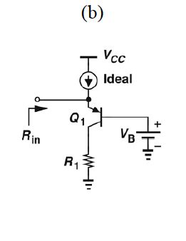
Input impedance refers to the effective resistance and reactance that a circuit presents to a signal source connected to its input terminals. It is a critical parameter in electrical and electronic systems, as it determines how much power is transferred from the source to the load, and how the circuit interacts with other components in the system.
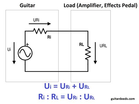
In general, the input impedance of a circuit should be matched to the output impedance of the source to ensure maximum power transfer and minimize signal reflections. This is especially important in high-frequency applications, such as radio and microwave systems, where impedance mismatches can cause significant signal loss and distortion.
Factors Affecting Input Impedance
The input impedance of a circuit depends on several factors, including:
- The circuit topology and components used
- The frequency of the input signal
- The load impedance connected to the output of the circuit
- Any parasitic capacitances or inductances present in the circuit
To optimize the input impedance of a circuit, designers must carefully select components and layout techniques that minimize parasitics and provide the desired impedance characteristics over the operating frequency range.
Transmission Lines and Their Role in Input Impedance Matching
Transmission lines are specialized cables or printed circuit board (PCB) traces designed to carry high-frequency signals with minimal loss and distortion. They are characterized by their characteristic impedance (Z0), which is determined by the geometry and materials of the conductors and dielectric.
Types of Transmission Lines
There are several common types of transmission lines used in electronic systems:
| Type | Characteristic Impedance (Z0) | Applications |
|---|---|---|
| Coaxial Cable | 50Ω, 75Ω | RF, Video |
| Microstrip | 50Ω, 75Ω, 100Ω | PCB traces |
| Stripline | 50Ω, 75Ω, 100Ω | PCB traces |
| Twisted Pair | 100Ω, 120Ω | Ethernet, Telephone |
To minimize reflections and ensure proper signal propagation, the characteristic impedance of the transmission line should match the input impedance of the load circuit. This is achieved through impedance matching techniques, such as using Quarter-wave transformers or stub matching.
Quarter-Wave Transformers
A quarter-wave transformer is a section of transmission line with a length equal to one-quarter wavelength (λ/4) of the signal frequency. Its characteristic impedance (Z1) is designed to match the input impedance of the load (ZL) to the source impedance (ZS) according to the following equation:
Z1 = √(ZS × ZL)
By inserting a quarter-wave transformer between the source and load, the input impedance seen by the source becomes equal to ZS, resulting in maximum power transfer and minimal reflections.
Stub Matching
Stub matching involves adding a short or open-circuited section of transmission line (stub) at a specific distance from the load to cancel out any reactive components of the input impedance. The length and characteristic impedance of the stub are chosen to create a purely resistive input impedance equal to the source impedance.
There are two main types of stub matching:
-
Single-stub matching: A single stub is used to cancel the reactive component of the load impedance. The stub is placed at a distance d from the load, where d is calculated based on the wavelength and the load impedance.
-
Double-stub matching: Two stubs are used to provide a wider bandwidth and greater flexibility in matching complex load impedances. The stubs are placed at specific distances from each other and the load, with their lengths and characteristic impedances optimized for the desired frequency range.

Input Impedance Matching Circuits
In addition to transmission line techniques, there are several lumped-element circuits commonly used for input impedance matching. These circuits use combinations of resistors, capacitors, and inductors to transform the load impedance to match the source impedance.
L-Network
An L-network is a simple matching circuit consisting of two reactive components (one inductor and one capacitor) arranged in an L-shape. The component values are chosen to cancel out the reactive part of the load impedance and transform the resistive part to match the source impedance.
L-networks are narrowband and can only match impedances with a limited range of resistive and reactive values. They are commonly used in low-frequency applications, such as audio and power electronics.
Pi-Network and T-Network
Pi-networks and T-networks are more complex matching circuits that use three reactive components to provide a wider matching range and bandwidth compared to L-networks. Pi-networks have two shunt components and one series component, while T-networks have two series components and one shunt component.
These networks can match a wider range of impedances and are often used in radio frequency (RF) applications, such as antenna matching and power amplifier output matching.
Transformers
Transformers can also be used for impedance matching by exploiting the relationship between the number of turns in the primary and secondary windings. The impedance transformation ratio of a transformer is given by:
(ZP / ZS) = (NP / NS)^2
Where:
– ZP is the primary impedance
– ZS is the secondary impedance
– NP is the number of turns in the primary winding
– NS is the number of turns in the secondary winding
By choosing the appropriate turns ratio, a transformer can match the source impedance to the load impedance while providing electrical isolation and voltage/current scaling. Transformers are commonly used in audio, power, and RF applications.

Designing Input Impedance Matching Circuits
When designing an input impedance matching circuit, several factors must be considered to ensure optimal performance:
-
Frequency range: The matching circuit must provide the desired impedance transformation over the entire operating frequency range of the system.
-
Bandwidth: The bandwidth of the matching circuit should be wide enough to accommodate any variations in the source or load impedance due to manufacturing tolerances or environmental factors.
-
Power handling: The components used in the matching circuit must be rated for the expected power levels to avoid overheating or damage.
-
Insertion loss: The matching circuit should introduce minimal insertion loss to maintain signal integrity and efficiency.
-
Size and cost: The matching circuit should be as compact and cost-effective as possible while still meeting the performance requirements.
To design an input impedance matching circuit, follow these steps:
- Determine the source and load impedances at the desired frequency range.
- Select a matching circuit topology (e.g., L-network, Pi-network, transformer) based on the required bandwidth, power handling, and impedance transformation ratio.
- Calculate the component values using impedance matching equations or simulation software.
- Simulate the circuit to verify its performance and optimize the component values if necessary.
- Build and test a prototype of the matching circuit to validate its real-world performance.

FAQ
Q1: What is the difference between input impedance and output impedance?
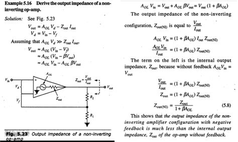
A1: Input impedance refers to the impedance that a circuit presents to a signal source connected to its input terminals, while output impedance refers to the impedance that a circuit presents to a load connected to its output terminals. In general, the output impedance of a source should be matched to the input impedance of the load for maximum power transfer and minimal signal reflections.
Q2: Why is impedance matching important in RF and microwave systems?
A2: In high-frequency systems, such as RF and microwave, impedance mismatches between the source, transmission line, and load can cause significant signal reflections, leading to power loss, signal distortion, and standing waves. By matching the impedances at each interface, these issues can be minimized, ensuring efficient power transfer and signal integrity.
Q3: What are the advantages of using transmission line matching techniques compared to lumped-element circuits?
A3: Transmission line matching techniques, such as quarter-wave transformers and stub matching, offer several advantages over lumped-element circuits:
1. They can handle higher power levels and frequencies due to their distributed nature and lack of discrete components.
2. They can provide a wider bandwidth and better impedance matching over a larger frequency range.
3. They can be easily integrated into PCB designs using microstrip or stripline traces.
However, transmission line techniques require more space and are generally more complex to design and optimize compared to lumped-element circuits.
Q4: How do you determine the characteristic impedance of a transmission line?
A4: The characteristic impedance of a transmission line depends on its geometry and the properties of the conductors and dielectric materials used. For common Transmission Line Types, such as coaxial cable or microstrip, the characteristic impedance can be calculated using the following equations:
Coaxial cable:
Z0 = (138 / √ε) × log(D / d)
Microstrip:
Z0 = (87 / √(εr + 1.41)) × ln(5.98H / (0.8W + T))
Where:
– ε is the dielectric constant of the insulating material
– εr is the relative dielectric constant of the substrate
– D is the inner diameter of the outer conductor
– d is the outer diameter of the inner conductor
– H is the substrate thickness
– W is the width of the microstrip trace
– T is the thickness of the microstrip trace
For more complex geometries or materials, electromagnetic simulation software can be used to accurately determine the characteristic impedance.
Q5: What are some common applications of input impedance matching circuits?
A5: Input impedance matching circuits are used in a wide range of applications, including:
-
RF and microwave systems: Impedance matching is critical in high-frequency systems to ensure efficient power transfer and minimize signal reflections. Examples include antenna matching, power amplifier input and output matching, and filter design.
-
Audio systems: Input impedance matching is important in audio systems to optimize signal transfer between components, such as microphones, preamplifiers, and power amplifiers. Proper matching ensures maximum power transfer, minimal noise, and flat frequency response.
-
Power electronics: In power conversion systems, such as switch-mode power supplies and motor drives, input impedance matching is used to minimize harmonic distortion, reduce electromagnetic interference (EMI), and improve overall efficiency.
-
Sensor and measurement systems: Impedance matching is crucial in sensor and measurement applications to maximize signal-to-noise ratio, minimize loading effects, and ensure accurate readings. Examples include bridge circuits, strain gauges, and thermocouple amplifiers.
By understanding the principles of input impedance and applying appropriate matching techniques, engineers and technicians can optimize the performance, efficiency, and reliability of a wide range of electronic systems.

No responses yet