What is Photoresist?
Photoresist is a light-sensitive material that is applied to the surface of a PCB during the fabrication process. It is composed of a polymer resin, a photosensitive compound, and a solvent. When exposed to light (typically UV light), the photoresist undergoes a chemical change, either becoming more soluble (positive photoresist) or less soluble (negative photoresist) in a developer solution.
There are two main types of photoresist:
-
Dry Film Photoresist: This type of photoresist comes in the form of a thin, dry film that is laminated onto the PCB surface using heat and pressure.
-
Liquid Photoresist: Liquid photoresist is applied to the PCB surface through various methods, such as spin coating, dip coating, or spraying.
In this article, we will focus on the spray photoresist method.
Why Use Spray Photoresist?
Spray photoresist offers several advantages over other application methods:
-
Even Coverage: Spraying ensures a uniform and consistent photoresist layer across the entire PCB surface, even on boards with complex geometries or large areas.
-
Adjustable Thickness: By controlling the spraying parameters, such as the distance from the PCB, the pressure, and the number of passes, you can achieve the desired photoresist thickness.
-
Fast Application: Spraying is a relatively quick process compared to other methods, making it suitable for high-volume production.
-
Cost-effective: Spray photoresist is an economical choice for small-scale or prototype production, as it requires less equipment and materials compared to dry film photoresist.
Materials and Equipment
To spray photoresist on PCBs, you will need the following materials and equipment:
-
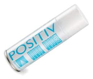
Liquid Photoresist: Choose a photoresist suitable for spraying, such as Positiv 20, KPR, or SUN-120.
-
Spray Gun: Use a spray gun specifically designed for photoresist application, such as the Wagner PCB Spray Gun or the Richon RP-100.
-
Compressed Air Source: You will need a clean, oil-free compressed air source to operate the spray gun. An air compressor or a compressed air canister can be used.
-
Ventilated Workspace: Spraying should be done in a well-ventilated area or a fume hood to minimize exposure to photoresist fumes.
-
Protective Gear: Wear appropriate personal protective equipment (PPE), such as gloves, safety glasses, and a respirator, to avoid contact with the photoresist and inhaling fumes.
-
PCB Cleaning Supplies: Before spraying, the PCB surface must be cleaned thoroughly. You will need isopropyl alcohol (IPA), lint-free wipes, and an anti-static brush.
-
UV Exposure Unit: After spraying, the photoresist-coated PCB will need to be exposed to UV light using an exposure unit.
-
Developer Solution: A developer solution is used to remove the unexposed photoresist after UV exposure. Choose a developer compatible with your photoresist.

Preparing the PCB Surface
Before applying the spray photoresist, it is essential to clean the PCB surface thoroughly to ensure proper adhesion and to avoid contamination. Follow these steps:
-
Mechanical Cleaning: Use an anti-static brush to remove any dust, debris, or loose particles from the PCB surface.
-
Chemical Cleaning: Dip a lint-free wipe in isopropyl alcohol (IPA) and gently wipe the PCB surface in a single direction to remove any grease, oils, or fingerprints. Allow the PCB to air dry completely.
-
Inspect the Surface: Visually inspect the PCB surface for any remaining contaminants or defects. Repeat the cleaning process if necessary.
Spraying Photoresist
Once the PCB surface is clean and dry, you can proceed with spraying the photoresist. Follow these steps:
-
Set Up the Workspace: Ensure that your workspace is well-ventilated and free from dust and debris. Place the PCB on a clean, flat surface.
-
Prepare the Spray Gun: Fill the spray gun reservoir with the liquid photoresist. Adjust the spray gun settings according to the manufacturer’s recommendations, such as the nozzle size, air pressure, and fluid flow rate.
-
Test the Spray Pattern: Before spraying the PCB, test the spray pattern on a piece of scrap material to ensure that the gun is working correctly and the pattern is uniform.
-
Apply the Photoresist: Hold the spray gun perpendicular to the PCB surface at a distance of about 15-20 cm (6-8 inches). Begin spraying from one edge of the PCB and move the gun in a smooth, steady motion, overlapping each pass by about 50%. Apply multiple thin coats rather than a single thick coat to achieve a uniform thickness.
-
Check the Thickness: Use a thickness gauge or a profilometer to measure the photoresist thickness. Aim for a thickness of 1-2 μm for most applications. If necessary, apply additional coats to achieve the desired thickness.
-
Allow to Dry: Let the sprayed PCB air dry for about 10-15 minutes, or use a low-temperature oven (around 50°C/122°F) to speed up the drying process.
UV Exposure and Development
After the photoresist has dried, the next steps are UV exposure and development:
-
Place the PCB in the Exposure Unit: Position the PCB with the photoresist side facing the UV light source. Ensure that the PCB is in close contact with the photomask or artwork.
-
Expose the Photoresist: Turn on the UV light source and expose the PCB for the recommended time, which depends on the photoresist type, thickness, and the exposure unit’s intensity. Consult the photoresist manufacturer’s datasheet for specific exposure times.
-
Develop the Photoresist: After exposure, immerse the PCB in the developer solution and gently agitate it for the specified development time. The unexposed photoresist will dissolve in the developer, leaving behind the desired circuit pattern.
-
Rinse and Dry: Rinse the developed PCB with water to stop the development process and remove any remaining developer. Gently blow dry the PCB with compressed air or let it air dry.
-
Inspect the PCB: Visually inspect the PCB under a microscope to ensure that the circuit pattern is complete, and there are no defects or undeveloped areas. If necessary, repeat the exposure and development process.
Best Practices
To achieve the best results when spraying photoresist on PCBs, consider the following best practices:
-
Maintain a Clean Environment: Keep your workspace clean and free from dust, debris, and contaminants to avoid defects in the photoresist layer.
-
Use Fresh Photoresist: Ensure that the photoresist is within its expiration date and has been stored properly to maintain its quality and performance.
-
Control the Spraying Parameters: Adjust the spraying parameters, such as the air pressure, fluid flow rate, and nozzle size, to achieve a uniform and consistent photoresist layer.
-
Apply Multiple Thin Coats: Instead of applying a single thick coat, apply multiple thin coats of photoresist to achieve a uniform thickness and avoid drips or runs.
-
Monitor the Thickness: Regularly measure the photoresist thickness using a thickness gauge or profilometer to ensure that it meets the required specifications.
-
Follow Safety Precautions: Always wear appropriate personal protective equipment (PPE) and work in a well-ventilated area to minimize exposure to photoresist fumes and chemicals.
-
Optimize the Exposure and Development: Follow the photoresist manufacturer’s recommendations for exposure time and development to achieve the best results. Optimize these parameters through trial and error if necessary.
Frequently Asked Questions (FAQ)
-
What is the ideal photoresist thickness for PCBs?
The ideal photoresist thickness depends on the specific application and the PCB’s features. For most standard PCBs, a thickness of 1-2 μm is sufficient. However, for high-resolution or fine-pitch designs, a thinner layer (around 0.5-1 μm) may be required. -
Can I use a regular spray gun for applying photoresist?
While it is possible to use a regular spray gun, it is not recommended. Photoresist spray guns are specially designed to provide precise control over the spraying parameters and ensure a uniform coating. Using a regular spray gun may result in an inconsistent layer thickness, overspray, or contamination. -
How can I remove the photoresist after etching?
After etching, the remaining photoresist can be removed using a photoresist stripper solution, such as acetone or a dedicated commercial stripper. Immerse the PCB in the stripper solution and agitate it gently until the photoresist dissolves completely. Rinse the PCB with water and dry it thoroughly. -
What should I do if the photoresist is too thick or too thin?
If the photoresist is too thick, you can reduce the number of coats applied or increase the distance between the spray gun and the PCB. If the photoresist is too thin, apply additional coats until the desired thickness is achieved. Always allow sufficient drying time between coats. -
Can I reuse the liquid photoresist?
It is generally not recommended to reuse liquid photoresist, as it may have been contaminated during the spraying process or have started to degrade due to exposure to air or light. Always use fresh photoresist for the best results and to avoid defects in the final PCB.
Conclusion
Spraying photoresist on PCBs is a critical step in the PCB Fabrication process, as it enables the transfer of the desired circuit pattern onto the copper surface. By following the proper procedures, using the right materials and equipment, and adhering to best practices, you can achieve a uniform and consistent photoresist layer that will result in high-quality PCBs.
Remember to always prioritize safety, maintain a clean working environment, and optimize the spraying, exposure, and development parameters to suit your specific requirements. With practice and experience, spraying photoresist will become a reliable and efficient method for your PCB fabrication needs.
No responses yet