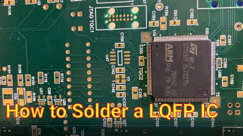
What is QFP Solder Bridging?
QFP, which stands for Quad Flat Package, is a surface-mounted integrated circuit package with leads extending from each of the four sides. QFP packages are very common in electronics manufacturing. However, their high pin density and fine lead pitch makes them prone to solder bridging defects.
Solder bridging occurs when solder inadvertently connects adjacent leads, creating an unintended short circuit. On QFP packages with many pins and narrow spaces between leads, solder paste can easily slump during reflow and join neighboring pins. QFP bridging is one of the most common solder defects in SMT assembly.
Why is QFP Bridging a Problem?
QFP solder bridges create unwanted short circuits that can prevent the circuit from functioning properly. Even if the device initially passes testing, latent QFP solder bridges may eventually lead to intermittent failures and reduced reliability in the field. Rework to remove QFP bridges is time-consuming and expensive. In severe cases, the entire board may need to be scrapped.
Some of the negative impacts of QFP solder bridging include:
- Device malfunction or complete failure
- Increased manufacturing costs due to rework
- Lower production yields
- Potential reliability issues and product returns
- Damage to the company’s reputation
Reducing QFP bridging is therefore critical to improving manufacturing quality and efficiency while avoiding costly defects that can harm the bottom line. Systematic defect prevention is always preferable to relying on detection and rework.
Common Causes of QFP Solder Bridging
To effectively prevent solder bridges, it’s important to understand the underlying causes. QFP bridging can stem from issues with the PCB design, stencil, solder paste, component placement, or reflow profile.
Some of the most frequent causes of QFP solder bridging include:
Improper Solder Paste Volume
Applying too much solder paste is a common cause of bridging on fine-pitch QFPs. Excessive solder paste increases the risk of paste slumping and solder wicking up the vertical sides of the leads.
Potential sources of excess paste include:
- Stencil apertures that are oversized or improperly shaped
- Worn or damaged stencils that allow scooping
- Squeegee pressure and speed settings that are too high
- Insufficient stencil cleaning frequency
Poor Paste Release from Stencil
If the solder paste doesn’t cleanly release from the stencil apertures, it can stick to the sides or bottom of the stencil. This results in insufficiently sized or malformed paste deposits that are prone to bridging.
Factors that can impede proper paste release include:
- Improperly sized or shaped stencil apertures
- Rough or unpolished stencil surfaces
- Solder paste that is too cold or has the wrong viscosity
- Insufficient snap-off distance between stencil and PCB
- PCB pads with inadequate soldermask clearance
Incorrect Component Placement
Misaligned or rotated QFP packages change the intended spatial relationship between leads and solder paste deposits. Even slight placement errors can significantly increase the risk of solder bridges forming.
Component placement issues often result from:
- Nozzles or pickup surfaces that are worn or dirty
- Incorrectly programmed placement pressure/height settings
- Inadequate fiducial recognition during alignment
- PCB support issues allowing board flex
- Vibrations or jolts disturbing placed components
Suboptimal Reflow Profile
An improper reflow profile can allow the solder paste to slump excessively before the alloy melts and coalesces on the pads and leads. Profiles with an overly long soak time, hot spots, or insufficient TAL are especially problematic.
Reflow profile issues are frequently caused by:
- Oven recipes not optimized for the board design
- Changed paste composition or powder size
- Insufficient profiling on each new setup
- Lack of oven verification and calibration
- Atmospheric anomalies impacting heat transfer

Strategies to Minimize QFP Solder Bridging
Solving QFP solder bridging requires a systematic approach that addresses paste volume, stencil quality, component placement, and the reflow profile. Implement the following strategies to minimize bridging and improve production yield:
1. Optimize Solder Paste Deposits
Proper control of solder paste volume is essential for QFP soldering. Strive for paste deposits that are sufficiently sized to form robust solder joints but not so large as to encourage bridging.
Guidelines for optimizing QFP solder paste deposits:
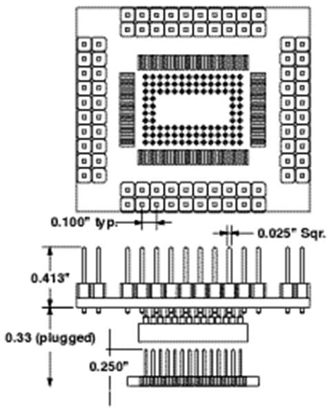
- Size stencil apertures at 80-90% of pad width
- Use a stencil thickness of 100-125 μm for fine-pitch QFPs
- Avoid aperture designs that promote clogging
- Round off aperture corners to facilitate paste release
- Utilize variable aperture sizes to equalize solder volumes
| QFP Pitch | Pad Width | Aperture Size | Stencil Thickness |
|---|---|---|---|
| 0.5 mm | 0.25 mm | 0.20-0.22 mm | 100 μm |
| 0.4 mm | 0.20 mm | 0.16-0.18 mm | 100 μm |
| 0.3 mm | 0.15 mm | 0.12-0.14 mm | 100-125 μm |
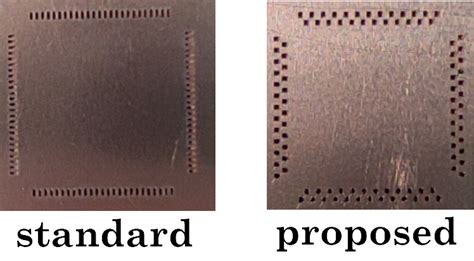
2. Maintain High Stencil Quality
Consistent, high-quality stencils are critical for controlling solder paste deposition on QFP lands. Even minor stencil issues can significantly impact paste release.
Best practices for ensuring excellent stencil quality:
- Opt for laser-cut or electroformed stencils over chemically etched
- Specify high-grade stencil materials like fine-grain stainless steel
- Insist on smooth aperture walls with 1.25-1.5 μm Ra finish
- Verify aperture dimensions and wall geometry for every stencil
- Implement a frequent stencil cleaning regimen tailored to paste type
- Train printers to look for stencil damage and clogged apertures
3. Tighten Component Placement Accuracy
Precise placement is essential for QFP packages, especially those with high lead counts and fine pitch. Strive for placement accuracy of at least ±50 μm.
Tips for improving QFP placement accuracy:
- Select a placement machine with fine-pitch QFP capability
- Utilize nozzles and pickup surfaces matched to component size
- Optimize placement force and height settings for each component
- Implement post-print PCB clamping to minimize board flex
- Dial in fiducial recognition parameters to ensure proper alignment
- Maintain the placement machine to avoid nozzle/jaws wear or dirt buildup
4. Develop the Optimal Reflow Profile
A well-designed reflow profile minimizes QFP solder bridging by allowing volatiles to escape and activating the flux before significant paste slump occurs. The peak temperature and time above liquidus should be high enough for proper coalescence but not so high as to promote excessive wetting.
Guidelines for developing a reflow profile that reduces QFP bridging:
- Use the paste manufacturer’s recommended profile as a starting point
- Minimize the time between 150-180°C to reduce paste slumping
- Set the peak temperature 10-20°C above solder liquidus point
- Limit time above liquidus to 60-90 seconds for lead-free solder
- Incorporate a controlled cool down rate of 2-4°C per second
- Perform periodic profile verification to check accuracy and repeatability
| Profile Parameter | Recommendation |
|---|---|
| Soak Time | 60-120 sec |
| Soak Temp | 150-180°C |
| Peak Temp | Liquidus + 10-20°C |
| Time Above Liquidus | 60-90 sec |
| Cooling Rate | 2-4°C/sec |
5. Address PCB Design Issues
Certain PCB design choices can make a QFP package more prone to solder bridging. Collaborate with the design team to ensure new designs are optimized for manufacturing.
PCB design tips to minimize QFP bridging:
- Size the pads to be 0.2-0.3 mm wider than the QFP leads
- Provide at least 0.15 mm of soldermask clearance around pads
- Avoid using soldermask between pads whenever possible
- Maximize distance between perimeter pads and package edge
- Ensure adequate routing space between pads for signal traces
- Incorporate PCB Tooling Holes to minimize board flex during processing
Frequently Asked Questions
What is the most common cause of QFP solder bridging?
Applying too much solder paste is the most frequent cause of QFP solder bridging. Excessive paste volume greatly increases the risk of slump bridging during reflow.
Is a nitrogen reflow atmosphere necessary to minimize QFP bridging?
While nitrogen can reduce solder oxidation and improve wetting, it is not required to minimize QFP bridging. Proper control of the paste volume and reflow profile have a larger impact.
What is an acceptable level of QFP solder bridging?
Most manufacturers strive for a QFP bridging rate of less than 100 defects per million opportunities (DPMO). However, the acceptable defect rate depends on the industry and product requirements.
Can solder bridges be repaired?
Yes, QFP solder bridges can often be repaired by carefully removing the excess solder with solder wick and flux. However, rework is time-consuming and can damage the PCB or components if not done properly.
How can you detect QFP solder bridges?
QFP solder bridges are typically detected via visual inspection under magnification after reflow. Automated optical inspection (AOI) equipment can also detect bridges but may struggle with false positives and negatives.
Conclusion
QFP solder bridging is a common defect that can seriously impact product quality and manufacturing efficiency. Implementing the strategies outlined in this article will help you significantly reduce solder bridging and improve first pass yield.
Remember, solder bridging is impacted by a wide range of inputs, from the PCB and stencil design to the solder paste and reflow profile. Regularly review each process step and verify that parameters are optimized for the specific board design. Continuous improvement efforts and ongoing defect monitoring are key to keeping QFP solder bridging under control.
No responses yet