Introduction to PCB Manufacturing
Printed Circuit Boards (PCBs) are the backbone of modern electronics. They are used in almost every electronic device, from smartphones and computers to industrial equipment and medical devices. PCB manufacturing is a complex process that involves several steps, each of which requires precision and attention to detail. In this article, we will explore the process of manufacturing small circuit boards, also known as PCBs.
What is a PCB?
A PCB is a flat board made of insulating material, such as fiberglass or plastic, with conductive copper traces printed on one or both sides. These traces connect electronic components, such as resistors, capacitors, and integrated circuits, to form a complete circuit. PCBs are used to mechanically support and electrically connect electronic components using conductive pathways, tracks, or signal traces etched from copper sheets laminated onto a non-conductive substrate.
Types of PCBs
There are several types of PCBs, each with its own unique characteristics and applications. The most common types of PCBs are:
-
Single-sided PCBs: These PCBs have conductive traces on only one side of the board. They are the simplest and cheapest type of PCB and are used in low-complexity electronic devices.
-
Double-sided PCBs: These PCBs have conductive traces on both sides of the board, which are connected through holes drilled in the board. They are more complex and expensive than single-sided PCBs and are used in more advanced electronic devices.
-
Multi-layer PCBs: These PCBs have multiple layers of conductive traces, separated by insulating layers. They are the most complex and expensive type of PCB and are used in high-performance electronic devices, such as smartphones and computers.

PCB Manufacturing Process
The PCB manufacturing process involves several steps, each of which requires specialized equipment and expertise. The main steps in the PCB manufacturing process are:
1. PCB Design
The first step in PCB manufacturing is to design the circuit board. This involves creating a schematic diagram of the circuit, which shows the electrical connections between the components. The schematic is then used to create a PCB layout, which shows the physical placement of the components on the board and the routing of the conductive traces.
There are several software tools available for PCB design, such as Altium Designer, Eagle, and KiCad. These tools allow designers to create complex PCB layouts quickly and accurately.
2. PCB Fabrication
Once the PCB design is complete, the next step is to fabricate the board. This involves several sub-steps, including:
2.1 PCB Material Selection
The first step in PCB fabrication is to select the appropriate material for the board. The most common materials used for PCBs are:
-
FR-4: This is a fiberglass-reinforced epoxy laminate that is the most widely used material for PCBs. It has good mechanical and electrical properties and is relatively cheap.
-
Polyimide: This is a high-performance plastic that is used in PCBs for aerospace and military applications. It has excellent thermal and chemical resistance but is more expensive than FR-4.
-
Aluminum: This is used in PCBs for high-power applications, such as LED lighting and motor controls. It has excellent thermal conductivity but is more expensive than FR-4.
2.2 PCB Lamination
The next step is to laminate the PCB material with a layer of copper on one or both sides. This is done by applying heat and pressure to the material in a lamination press. The copper layer is typically 1 oz. (35 μm) or 2 oz. (70 μm) thick.
2.3 PCB Drilling
After lamination, the next step is to drill holes in the board for the components and vias. This is done using a CNC drilling machine, which can drill holes as small as 0.1 mm in diameter with high precision.
2.4 PCB Plating
The holes drilled in the previous step are then plated with a conductive material, typically copper, to create electrical connections between the layers of the board. This is done using a process called electroplating, where the board is immersed in a plating solution and an electric current is applied to deposit the copper onto the walls of the holes.
2.5 PCB etching
The next step is to remove the unwanted copper from the board, leaving only the desired conductive traces. This is done using a process called etching, where the board is exposed to a chemical solution that dissolves the copper. The most common etching methods are:
-
Subtractive etching: This involves applying a photoresist layer to the board, exposing it to light through a photomask, and then developing the photoresist to create a pattern of the desired traces. The board is then immersed in an etching solution, which removes the copper from the areas not protected by the photoresist.
-
Additive etching: This involves applying a thin layer of copper to the entire board and then selectively plating additional copper onto the desired traces using a process called electrolytic plating.
2.6 PCB Solder Mask Application
After etching, a solder mask layer is applied to the board to protect the copper traces from oxidation and to prevent solder bridging during the assembly process. The solder mask is typically green in color but can also be yellow, red, blue, or black.
2.7 PCB Silkscreen Printing
The final step in PCB fabrication is to print the component labels and other markings onto the board using a silkscreen printing process. This involves applying a thin layer of ink to the board through a fine mesh screen.
3. PCB Assembly
After the PCB is fabricated, the next step is to assemble the components onto the board. This involves several sub-steps, including:
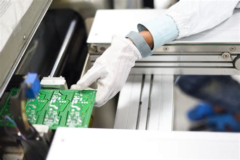
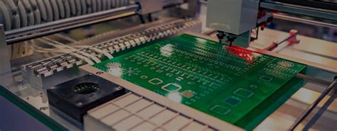
3.1 Component Placement
The first step in PCB assembly is to place the components onto the board. This is typically done using a pick-and-place machine, which uses a vacuum nozzle to pick up the components from a reel or tray and place them onto the board with high precision.
3.2 Soldering
After the components are placed, they are soldered onto the board using one of several methods, including:
-
Wave soldering: This involves passing the board over a wave of molten solder, which flows over the components and creates electrical connections.
-
Reflow soldering: This involves applying a solder paste to the board and then heating the board in a reflow oven to melt the solder and create electrical connections.
-
Hand soldering: This involves manually soldering the components onto the board using a soldering iron.
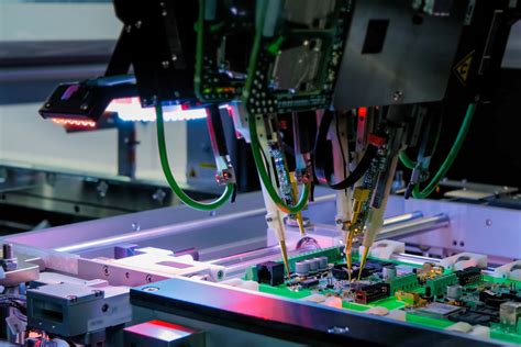
3.3 Inspection and Testing
After soldering, the board is inspected and tested to ensure that it is functioning properly. This involves several methods, including:
-
Visual inspection: This involves manually inspecting the board for any visible defects, such as solder bridges or missing components.
-
Automated optical inspection (AOI): This involves using a camera to scan the board and compare it to a reference image to identify any defects.
-
In-circuit testing (ICT): This involves using a test fixture to make electrical contact with the board and test each component individually.
-
Functional testing: This involves testing the board in its final application to ensure that it is functioning properly.
4. PCB Finishing
After the PCB is assembled and tested, the final step is to apply any necessary finishes to the board. This can include:
-
Conformal coating: This involves applying a thin layer of protective coating to the board to protect it from moisture, dust, and other environmental factors.
-
Potting: This involves encapsulating the board in a resin or epoxy to protect it from vibration and shock.
-
Labeling: This involves applying labels or markings to the board for identification and traceability purposes.
PCB Manufacturing Considerations
When manufacturing PCBs, there are several important considerations to keep in mind, including:
1. Material Selection
The choice of PCB material can have a significant impact on the performance and reliability of the final product. Factors to consider when selecting a PCB material include:
-
Dielectric constant: This is a measure of the material’s ability to store electrical energy. A lower dielectric constant is desirable for high-frequency applications.
-
Thermal conductivity: This is a measure of the material’s ability to dissipate heat. A higher thermal conductivity is desirable for high-power applications.
-
Coefficient of thermal expansion (CTE): This is a measure of the material’s tendency to expand or contract with changes in temperature. A lower CTE is desirable to prevent warping or cracking of the board.
2. Design for Manufacturing (DFM)
When designing a PCB, it is important to consider the manufacturing process and design the board accordingly. This involves following certain design rules and guidelines, such as:
-
Minimum trace width and spacing: The minimum trace width and spacing depends on the manufacturing process and the capabilities of the PCB fabricator. Typical values are 0.1 mm for trace width and 0.1 mm for spacing.
-
Minimum hole size: The minimum hole size depends on the drilling process and the capabilities of the PCB fabricator. Typical values are 0.2 mm for mechanical drilling and 0.1 mm for laser drilling.
-
Solder mask and silkscreen clearance: The solder mask and silkscreen should be designed with sufficient clearance from the copper traces to prevent shorts or other defects.
3. Quality Control
Quality control is essential in PCB manufacturing to ensure that the final product meets the required specifications and performance requirements. This involves implementing several quality control measures, such as:
-
Incoming inspection: This involves inspecting the raw materials and components before they are used in the manufacturing process to ensure that they meet the required specifications.
-
In-process inspection: This involves inspecting the PCBs at various stages of the manufacturing process to identify any defects or issues.
-
Final inspection: This involves inspecting the finished PCBs to ensure that they meet the required specifications and performance requirements.
-
Traceability: This involves maintaining records of the materials, processes, and personnel involved in the manufacturing of each PCB to enable traceability in case of any issues or defects.
Advantages of PCB Manufacturing
PCB manufacturing offers several advantages over other methods of electronic circuit construction, including:
-
Reliability: PCBs are highly reliable and durable, with a longer lifespan than other methods of electronic circuit construction.
-
Consistency: PCBs are manufactured using automated processes, which ensures a high degree of consistency and repeatability.
-
Miniaturization: PCBs enable the miniaturization of electronic circuits, allowing for smaller and more compact devices.
-
Cost-effective: PCBs are cost-effective for high-volume production, as the cost per unit decreases with increasing volume.
Challenges in PCB Manufacturing
Despite the many advantages of PCB manufacturing, there are also several challenges that need to be addressed, including:
-
High initial setup costs: PCB manufacturing requires significant initial investment in equipment and facilities, which can be a barrier to entry for small businesses and startups.
-
Rapid technological changes: The electronics industry is constantly evolving, with new technologies and materials being introduced regularly. This requires PCB manufacturers to continuously adapt and invest in new equipment and processes.
-
Environmental concerns: PCB manufacturing involves the use of chemicals and materials that can be harmful to the environment if not properly managed. This requires PCB manufacturers to implement strict environmental controls and waste management practices.
-
Skilled labor shortage: PCB manufacturing requires skilled labor, such as engineers, technicians, and operators. However, there is a growing shortage of skilled labor in many countries, which can impact the quality and productivity of PCB manufacturing.
Future Trends in PCB Manufacturing
The PCB manufacturing industry is constantly evolving, with new technologies and trends emerging regularly. Some of the key trends in PCB manufacturing include:
-
Miniaturization: The trend towards miniaturization is expected to continue, with smaller and more compact PCBs being developed for a wide range of applications.
-
Flexible and stretchable PCBs: Flexible and stretchable PCBs are becoming increasingly popular, particularly in wearable electronics and medical devices.
-
3D printing: 3D printing is being explored as a potential method for PCB manufacturing, allowing for greater design freedom and faster prototyping.
-
Sustainable materials: There is a growing trend towards the use of sustainable materials in PCB manufacturing, such as biodegradable and recyclable materials.
Conclusion
PCB manufacturing is a complex process that requires specialized equipment, expertise, and attention to detail. When manufacturing small circuit boards, it is important to consider factors such as material selection, design for manufacturing, and quality control to ensure that the final product meets the required specifications and performance requirements. PCB manufacturing offers several advantages over other methods of electronic circuit construction, including reliability, consistency, miniaturization, and cost-effectiveness. However, there are also several challenges that need to be addressed, such as high initial setup costs, rapid technological changes, environmental concerns, and skilled labor shortages. As the electronics industry continues to evolve, the PCB manufacturing industry is expected to adapt and innovate to meet the changing needs and requirements of the market.
FAQs
-
What is the minimum trace width and spacing for PCBs?
The minimum trace width and spacing depends on the manufacturing process and the capabilities of the PCB fabricator. Typical values are 0.1 mm for trace width and 0.1 mm for spacing. -
What is the difference between single-sided and double-sided PCBs?
Single-sided PCBs have conductive traces on only one side of the board, while double-sided PCBs have conductive traces on both sides of the board. Double-sided PCBs are more complex and expensive than single-sided PCBs but offer more design flexibility and higher circuit density. -
What is the purpose of solder mask on PCBs?
The solder mask is a layer of insulating material that is applied to the surface of the PCB to protect the copper traces from oxidation and to prevent solder bridging during the assembly process. It also provides insulation between the copper traces and the components. -
What are the advantages of using flexible PCBs?
Flexible PCBs offer several advantages over rigid PCBs, including greater design flexibility, reduced weight and size, and improved reliability in applications that require bending or flexing. They are commonly used in wearable electronics, medical devices, and aerospace applications. -
What are the environmental concerns associated with PCB manufacturing?
PCB manufacturing involves the use of chemicals and materials that can be harmful to the environment if not properly managed. These include lead, which is used in solder, and various solvents and acids used in the manufacturing process. PCB manufacturers are required to implement strict environmental controls and waste management practices to minimize the environmental impact of their operations.
| PCB Type | Advantages | Disadvantages |
|---|---|---|
| Single-sided | Low cost, simple design | Limited circuit density, not suitable for complex designs |
| Double-sided | Higher circuit density, more design flexibility | Higher cost, more complex manufacturing process |
| Multi-layer | Highest circuit density, best for complex designs | Highest cost, most complex manufacturing process |
| PCB Material | Advantages | Disadvantages |
|---|---|---|
| FR-4 | Low cost, good mechanical and electrical properties | Limited thermal conductivity, not suitable for high-temperature applications |
| Polyimide | Excellent thermal and chemical resistance | High cost, limited availability |
| Aluminum | Excellent thermal conductivity | High cost, limited design flexibility |
No responses yet