Introduction to Multilayer PCB Manufacturing
Multilayer PCBs (Printed Circuit Boards) are essential components in modern electronics, enabling the creation of compact, high-performance devices. The manufacturing process of multilayer PCBs involves several intricate steps that require precision and expertise. In this article, we will delve into the details of multilayer PCB manufacturing, exploring the various stages involved and the technologies used to create these complex circuit boards.
What is a Multilayer PCB?
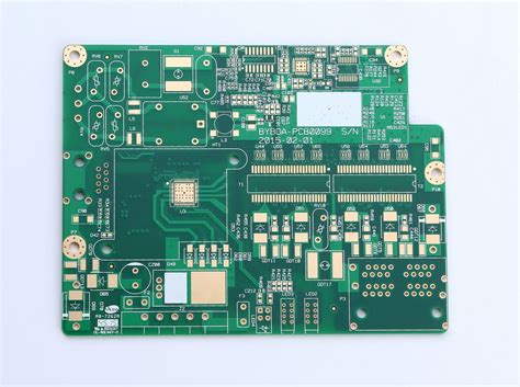
A multilayer PCB is a printed circuit board that consists of three or more conductive copper layers separated by insulating layers. These layers are laminated together to form a single board, allowing for higher component density and more complex circuit designs compared to single or double-layer PCBs. Multilayer PCBs are commonly used in applications that require high performance, reliability, and miniaturization, such as smartphones, computers, medical devices, and aerospace systems.
Advantages of Multilayer PCBs
- Increased circuit density and functionality
- Improved signal integrity and reduced electromagnetic interference (EMI)
- Enhanced thermal management and power distribution
- Reduced overall board size and weight
- Higher reliability and durability

The Multilayer PCB Manufacturing Process
The manufacturing process of multilayer PCBs involves several stages, each requiring specific equipment, materials, and expertise. The following sections will discuss each stage in detail.
Step 1: PCB Design and Layout
The first step in multilayer PCB manufacturing is designing the circuit layout using specialized PCB design software. The design process involves the following sub-steps:
- Schematic capture: Creating a graphical representation of the circuit’s components and their interconnections.
- Component placement: Arranging the components on the board to optimize space and minimize signal interference.
- Routing: Connecting the components using conductive traces while adhering to design rules and constraints.
- Design rule check (DRC): Verifying that the design meets the specified manufacturing and electrical requirements.
Step 2: Material Selection and Preparation
Once the PCB design is finalized, the appropriate materials for the board’s layers are selected. The most common materials used in multilayer PCB manufacturing are:
- Copper foil: Used for the conductive layers, typically with a thickness of 0.5 oz to 2 oz per square foot.
- Prepreg (pre-impregnated) material: A partially cured composite material used as an insulating layer between the copper layers.
- Core material: A fully cured dielectric material, such as FR-4, used as a base for the copper layers.
The selected materials are cut to the required sizes and cleaned to remove any contaminants that may affect the lamination process.
Step 3: Inner Layer Printing and Etching
The inner layers of the multilayer PCB are printed and etched using the following sub-steps:
- Applying a photoresist coating to the copper foil.
- Exposing the photoresist to UV light through a photomask containing the desired circuit pattern.
- Developing the photoresist to remove the unexposed areas, leaving the circuit pattern protected.
- Etching the unprotected copper using a chemical solution, typically cupric chloride or ammonium persulfate.
- Stripping the remaining photoresist to reveal the etched copper circuit pattern.
Step 4: Lamination
The inner layers, prepreg, and outer layers are aligned and stacked together in a specific order. The stack is then placed in a lamination press, where it is subjected to high pressure and temperature. The heat and pressure cause the prepreg to melt and flow, bonding the layers together to form a solid, multilayer board.
Step 5: Drilling
After lamination, holes are drilled through the board to accommodate through-hole components and create vias for inter-layer connections. The drilling process is performed using high-speed, computer-controlled drill machines that ensure precise hole placement and size.
Step 6: Plating and Copper Deposition
To establish electrical connections between layers, the drilled holes are plated with copper. This process involves the following sub-steps:
- Desmearing: Removing any resin smear from the hole walls to ensure proper copper adhesion.
- Electroless copper deposition: Applying a thin layer of copper to the hole walls using a chemical process.
- Electroplating: Depositing additional copper onto the electroless layer using an electric current to achieve the desired thickness.
Step 7: Outer Layer Printing and Etching
The outer layers of the multilayer PCB undergo a similar printing and etching process as the inner layers (described in Step 3). This step creates the final circuit pattern on the board’s surface.
Step 8: Solder Mask Application
A solder mask, typically a green or blue polymer coating, is applied to the outer layers of the PCB. The solder mask serves two primary purposes:
- Protecting the copper traces from oxidation and short-circuits.
- Providing a visual guide for component placement and soldering.
The solder mask is applied using a screen-printing process and then cured using UV light or heat.
Step 9: Surface Finish
To enhance the solderability and protect the exposed copper pads, a surface finish is applied. Common surface finishes include:
- HASL (Hot Air Solder Leveling): A thin layer of solder is applied to the pads and then leveled using hot air.
- ENIG (Electroless Nickel Immersion Gold): A layer of nickel is deposited onto the pads, followed by a thin layer of gold.
- OSP (Organic Solderability Preservative): A clear, organic compound is applied to the pads to prevent oxidation.
Step 10: Electrical Testing and Inspection
The manufactured multilayer PCBs undergo rigorous electrical testing and visual inspection to ensure they meet the required specifications and are free of defects. Some common testing methods include:
- Flying probe test: A set of probes is used to check the continuity and isolation of the circuit paths.
- In-circuit test (ICT): The PCB is placed in a fixture with pins that contact specific points on the board to verify the presence and correct function of components.
- Automated optical inspection (AOI): A camera-based system scans the PCB for visual defects, such as solder bridges or missing components.
Step 11: Finishing and Packaging
After testing and inspection, the multilayer PCBs are cut to their final dimensions using a routing machine or a laser cutter. The boards are then cleaned, labeled, and packaged for shipment to the customer.

Challenges in Multilayer PCB Manufacturing
While multilayer PCBs offer numerous advantages, their manufacturing process presents several challenges:
- Achieving precise alignment between layers during lamination
- Maintaining consistent dielectric thickness and impedance control
- Minimizing signal integrity issues, such as crosstalk and signal attenuation
- Ensuring reliable inter-layer connections through vias
- Managing thermal expansion and contraction during the manufacturing process
To overcome these challenges, manufacturers employ advanced technologies, such as high-precision alignment systems, laser drilling, and 3D modeling software for PCB design and simulation.

Quality Control in Multilayer PCB Manufacturing
Maintaining high quality standards is crucial in multilayer PCB manufacturing to ensure the reliability and performance of the final product. Some key quality control measures include:
- Implementing a robust quality management system (QMS) based on industry standards, such as ISO 9001 or AS9100.
- Conducting regular process audits and equipment calibration to maintain consistency and accuracy.
- Utilizing statistical process control (SPC) techniques to monitor and optimize the manufacturing process.
- Performing thorough incoming material inspections to ensure the quality of raw materials.
- Conducting comprehensive electrical testing and visual inspection of the finished PCBs.
Future Trends in Multilayer PCB Manufacturing
As electronic devices continue to advance and miniaturize, multilayer PCB manufacturing technologies must evolve to keep pace. Some future trends in the industry include:
- Increasing the number of layers and reducing layer thickness to accommodate higher component density.
- Adopting advanced materials, such as high-frequency laminates and embedded components, to improve performance and functionality.
- Implementing 3D printing technologies for rapid prototyping and low-volume production.
- Developing environmentally friendly manufacturing processes and materials to reduce the industry’s ecological footprint.
- Integrating artificial intelligence (AI) and machine learning (ML) techniques to optimize PCB design and manufacturing processes.
Conclusion
Multilayer PCB manufacturing is a complex and multi-faceted process that involves numerous stages, each requiring specific expertise and technologies. By understanding the various steps involved in manufacturing multilayer PCBs, designers and engineers can create more efficient and reliable electronic devices. As the demand for high-performance, compact electronics continues to grow, the multilayer PCB industry will remain at the forefront of technological advancement, driving innovation across numerous sectors.
Frequently Asked Questions (FAQ)
1. What is the minimum number of layers required for a PCB to be considered a multilayer PCB?
A PCB must have at least three conductive layers to be classified as a multilayer PCB. This includes two outer layers and at least one inner layer.
2. What materials are commonly used for the insulating layers in multilayer PCBs?
The most common insulating materials used in multilayer PCBs are FR-4, a glass-reinforced epoxy laminate, and prepreg, a partially cured composite material made of glass cloth impregnated with a resin system.
3. How are the layers of a multilayer PCB connected electrically?
The layers of a multilayer PCB are connected electrically through vias, which are holes drilled through the board and plated with copper. Vias can be either through-holes, connecting all layers, or blind or buried vias, connecting only specific layers.
4. What is the purpose of the solder mask in multilayer PCB manufacturing?
The solder mask serves two main purposes: protecting the copper traces from oxidation and short-circuits, and providing a visual guide for component placement and soldering. It is typically a green or blue polymer coating applied to the outer layers of the PCB.
5. How can manufacturers ensure the reliability and quality of multilayer PCBs?
Manufacturers ensure the reliability and quality of multilayer PCBs by implementing robust quality control measures, such as conducting regular process audits, utilizing statistical process control techniques, performing thorough material inspections, and conducting comprehensive electrical testing and visual inspection of the finished PCBs.
Multilayer PCB Manufacturing Process Overview
| Step | Process | Description |
|---|---|---|
| 1 | PCB Design and Layout | Creating the circuit layout using specialized PCB design software |
| 2 | Material Selection and Preparation | Selecting and preparing the appropriate materials for the board’s layers |
| 3 | Inner Layer Printing and Etching | Printing and etching the circuit pattern on the inner layers |
| 4 | Lamination | Aligning and bonding the layers together using high pressure and temperature |
| 5 | Drilling | Creating holes for through-hole components and vias using computer-controlled drill machines |
| 6 | Plating and Copper Deposition | Establishing electrical connections between layers by plating the drilled holes with copper |
| 7 | Outer Layer Printing and Etching | Creating the final circuit pattern on the board’s surface |
| 8 | Solder Mask Application | Applying a protective polymer coating to the outer layers |
| 9 | Surface Finish | Enhancing the solderability and protecting the exposed copper pads |
| 10 | Electrical Testing and Inspection | Verifying the functionality and quality of the manufactured PCBs |
| 11 | Finishing and Packaging | Cutting the PCBs to their final dimensions, cleaning, labeling, and packaging for shipment |
No responses yet