Understanding High-Frequency PCB Design
Before diving into the specific design rules, it’s crucial to understand what constitutes a high-frequency PCB and why designing them requires special attention.
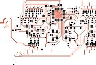
What is a High-Frequency PCB?
A high-frequency PCB is a printed circuit board designed to operate at frequencies typically above 100 MHz. At these frequencies, the behavior of signals on the PCB becomes more complex, and traditional design approaches may no longer be sufficient. High-frequency signals are more susceptible to issues such as signal integrity degradation, crosstalk, and EMI.
Challenges in High-Frequency PCB Design
Designing high-frequency PCBs presents several challenges that must be addressed to ensure optimal performance:
-
Signal Integrity: At high frequencies, signals are more prone to distortion, reflections, and losses due to factors such as impedance mismatches, parasitic capacitance, and inductance.
-
Electromagnetic Interference (EMI): High-frequency signals can generate unwanted electromagnetic radiation, causing interference with other components or systems. Proper shielding and grounding techniques are essential to minimize EMI.
-
Crosstalk: As signal frequencies increase, the coupling between adjacent traces becomes more significant, leading to crosstalk. Crosstalk can cause signal distortion and compromise the overall system performance.
-
Thermal Management: High-frequency components often generate more heat, requiring efficient thermal management strategies to prevent overheating and ensure reliable operation.
11 Design Rules for High-Frequency PCBs
To address the challenges associated with high-frequency PCB design, follow these 11 design rules:
1. Choose the Right Substrate Material
The choice of substrate material is crucial in high-frequency PCB design. The substrate’s dielectric constant (Dk) and dissipation factor (Df) directly impact signal propagation and losses. For high-frequency applications, consider using low-loss materials such as Rogers RO4000 series, PTFE (Teflon), or Isola TerraGreen. These materials have a stable Dk and low Df, minimizing signal distortion and losses.
2. Minimize Trace Length and Optimize Routing
Keep trace lengths as short as possible to reduce signal propagation delay and minimize losses. Avoid unnecessary bends and turns in the traces, as they can introduce impedance discontinuities and reflections. Use direct routing paths whenever possible, and if bends are necessary, use gentle curves instead of sharp 90-degree angles.
3. Control Impedance
Impedance Control is critical in high-frequency PCB design to ensure proper signal integrity. Determine the target impedance value based on the system requirements and design the traces accordingly. Use impedance calculators or simulation tools to determine the appropriate trace width, thickness, and spacing. Maintain consistent impedance throughout the signal path to minimize reflections and signal distortion.
4. Implement Proper Grounding Techniques
Proper grounding is essential for reducing EMI and ensuring a low-impedance return path for high-frequency signals. Use a solid ground plane whenever possible, as it provides a low-impedance reference for signals and helps reduce EMI. Avoid split ground planes or slots in the ground plane, as they can create impedance discontinuities and cause signal integrity issues.
5. Utilize Ground Stitching Vias
To maintain a continuous ground reference and minimize EMI, use ground stitching vias along the edges of the PCB and around sensitive components. Ground stitching vias help create a Faraday cage effect, containing electromagnetic fields within the PCB and reducing external interference. Place the vias at regular intervals, typically every λ/20 (one-twentieth of the wavelength) at the highest frequency of interest.
6. Implement Proper Decoupling and Bypassing
Decoupling and bypassing capacitors play a crucial role in maintaining power integrity and reducing noise in high-frequency PCBs. Place decoupling capacitors as close as possible to the power pins of high-frequency components to minimize the inductance in the power distribution network. Use a combination of bulk and ceramic capacitors to provide a low-impedance path for high-frequency noise.
7. Minimize Crosstalk
To minimize crosstalk between adjacent traces, follow these guidelines:
– Increase the spacing between traces, especially for long parallel runs.
– Use guard traces or ground shields between sensitive traces to reduce coupling.
– Avoid running high-speed traces parallel to each other for long distances.
– Consider using differential signaling for critical high-frequency signals, as it helps cancel out common-mode noise and reduces crosstalk.
8. Implement Shielding Techniques
Shielding is an effective way to reduce EMI and protect sensitive circuits from external interference. Use shielding cans or enclosures to isolate high-frequency components or sections of the PCB. Ensure proper grounding of the shields to the PCB ground plane. Additionally, consider using shielded connectors and cables for off-board connections to minimize EMI.
9. Optimize Component Placement
Proper component placement is crucial for minimizing signal path lengths, reducing crosstalk, and improving overall system performance. Place high-frequency components close to each other to minimize trace lengths and reduce propagation delays. Keep sensitive components away from noisy components or regions of the PCB. Consider the orientation of components to minimize coupling and interference.
10. Utilize High-Speed Design Techniques
Implement high-speed design techniques to optimize signal integrity and minimize signal distortion:
– Use differential signaling for critical high-frequency signals to reduce noise and improve signal quality.
– Implement impedance matching techniques, such as series termination or parallel termination, to minimize reflections and ensure proper signal termination.
– Consider using equalization techniques, such as pre-emphasis or de-emphasis, to compensate for high-frequency losses and improve signal quality over long traces.
11. Perform Thorough Simulation and Testing
Before finalizing the PCB design, perform thorough simulations to analyze signal integrity, EMI, and thermal performance. Use electromagnetic field solvers and Circuit Simulators to identify potential issues and optimize the design. After fabrication, conduct comprehensive testing to validate the PCB’s performance and ensure it meets the specified requirements. Perform signal integrity measurements, EMI tests, and thermal analysis to verify the design’s robustness.

FAQ
-
What is the importance of impedance control in high-frequency PCB design?
Impedance control is crucial in high-frequency PCB design to ensure proper signal integrity. By maintaining consistent impedance throughout the signal path, reflections and signal distortion are minimized, resulting in cleaner and more reliable signal transmission. -
How does the choice of substrate material affect high-frequency PCB Performance?
The choice of substrate material directly impacts signal propagation and losses in high-frequency PCBs. Low-loss materials with stable dielectric constant (Dk) and low dissipation factor (Df) are preferred for high-frequency applications. These materials minimize signal distortion and losses, ensuring better signal quality and performance. -
What is the purpose of ground stitching vias in high-frequency PCB design?
Ground stitching vias help maintain a continuous ground reference and minimize EMI in high-frequency PCBs. By placing vias along the edges of the PCB and around sensitive components at regular intervals, a Faraday cage effect is created, containing electromagnetic fields within the PCB and reducing external interference. -
How can crosstalk be minimized in high-frequency PCB design?
Crosstalk can be minimized in high-frequency PCB design by increasing the spacing between traces, using guard traces or ground shields, avoiding long parallel runs of high-speed traces, and considering differential signaling for critical high-frequency signals. These techniques help reduce coupling and interference between adjacent traces. -
Why is thorough simulation and testing important in high-frequency PCB design?
Thorough simulation and testing are essential in high-frequency PCB design to identify and address potential issues before finalizing the design. Simulations help analyze signal integrity, EMI, and thermal performance, allowing for design optimization. Comprehensive testing after fabrication validates the PCB’s performance and ensures it meets the specified requirements, minimizing the risk of costly rework or failures in the final application.

Conclusion
Designing high-frequency PCBs requires careful consideration of various factors to ensure optimal signal integrity, minimize EMI, and maintain overall system reliability. By following the 11 design rules outlined in this article, engineers can effectively navigate the challenges associated with high-frequency PCB design.
From choosing the right substrate material and controlling impedance to implementing proper grounding and shielding techniques, each design rule plays a crucial role in achieving a robust and reliable high-frequency PCB. Additionally, thorough simulation and testing are essential to validate the design and ensure it meets the stringent requirements of modern electronic applications.
By understanding and applying these design rules, engineers can create high-frequency PCBs that deliver exceptional performance, minimize signal integrity issues, and provide a solid foundation for the ever-increasing demands of high-speed electronic devices.

No responses yet