Introduction to Solder Paste Testing
Solder paste printing is a critical process in the manufacturing of printed circuit boards (PCBs). It involves depositing a precise amount of solder paste onto the PCB pads, which will later be used to establish electrical connections between components during the reflow soldering process. To ensure the quality and reliability of the final product, it is essential to test the solder paste printing process at various stages.
In this article, we will discuss the various methods and techniques used to test solder paste printing, including:
- Visual inspection
- Solder paste volume measurement
- Solder paste height measurement
- Solder paste area coverage measurement
- Solder paste slump testing
- Solder paste tackiness testing
- Solder paste viscosity testing
- Solder paste particle size analysis
- Solder paste flux activity testing
- Solder paste printing process optimization
We will also cover the importance of solder paste testing, the equipment used, and best practices to ensure consistent and reliable results.
Why is Solder Paste Testing Important?
Solder paste printing is a delicate process that requires precise control over various parameters such as stencil aperture size, paste viscosity, printing speed, and pressure. Any deviation from the optimal settings can lead to defects such as insufficient or excessive solder paste deposition, bridging, solder beads, or poor wetting.
These defects can cause a range of issues in the final product, including:
- Poor electrical connections
- Short circuits
- Open circuits
- Reduced mechanical strength
- Reduced reliability
- Increased rework and repair costs
By regularly testing the solder paste printing process, manufacturers can identify and correct any issues early in the production process, reducing the risk of defects and improving overall product quality.

Visual Inspection
Visual inspection is the most basic and commonly used method for testing solder paste printing. It involves examining the printed PCB under a microscope or magnifying glass to check for any visible defects or anomalies.
Some of the key aspects to look for during visual inspection include:
- Paste volume: Check if the solder paste deposit is sufficient to form a reliable connection during reflow soldering.
- Paste shape: Ensure that the solder paste deposit is uniform and has a consistent shape across all pads.
- Paste alignment: Verify that the solder paste is accurately aligned with the PCB pads and does not extend beyond the pad boundaries.
- Bridging: Look for any solder paste bridges between adjacent pads, which can cause short circuits.
- Solder beads: Check for any small solder beads or splashes around the pads, which can cause short circuits or other issues.
While visual inspection is a quick and easy method for identifying gross defects, it has some limitations:
- It is subjective and depends on the operator’s expertise and judgment.
- It cannot provide quantitative measurements of solder paste volume, height, or area coverage.
- It may not detect subtle defects or variations that can still impact the final product quality.

Solder Paste Volume Measurement
Solder paste volume measurement is a more precise and objective method for testing solder paste printing. It involves using specialized equipment to measure the volume of solder paste deposited on each pad.
There are two main types of solder paste volume measurement systems:
- 2D measurement systems: These systems use a camera to capture an image of the printed PCB and then use image processing algorithms to calculate the solder paste volume based on the area and height of each deposit. Some examples of 2D measurement systems include:
- Solder Paste Inspection (SPI) systems
- Automated Optical Inspection (AOI) systems
-
Vision-based measurement systems
-
3D measurement systems: These systems use a laser or structured light to scan the surface of the printed PCB and create a 3D map of the solder paste deposits. They can provide more accurate and detailed measurements of solder paste volume, height, and shape. Some examples of 3D measurement systems include:
- Laser profilometers
- Structured light scanners
- Confocal microscopes
Solder paste volume measurement systems typically provide the following metrics:
| Metric | Description |
|---|---|
| Volume | The total volume of solder paste deposited on each pad, measured in cubic millimeters (mm³) or nanoliters (nL) |
| Height | The maximum height of the solder paste deposit, measured in micrometers (µm) or mils |
| Area | The area of the solder paste deposit, measured in square millimeters (mm²) or square mils |
These metrics can be compared against predefined tolerances or specifications to determine if the solder paste printing process is within acceptable limits.

Solder Paste Height Measurement
Solder paste height measurement is a specific type of solder paste volume measurement that focuses on the maximum height of each solder paste deposit. It is important because the height of the solder paste can affect the reflow soldering process and the final solder joint quality.
If the solder paste height is too low, there may not be enough solder to form a reliable connection between the component and the PCB pad. This can lead to open circuits or weak solder joints that may fail under stress or vibration.
On the other hand, if the solder paste height is too high, it can cause bridging between adjacent pads or components, leading to short circuits or other defects.
Solder paste height measurement can be performed using the same equipment and techniques as solder paste volume measurement, such as 2D or 3D measurement systems.
The typical height range for solder paste deposits is between 100 and 200 µm (4 to 8 mils), depending on the stencil thickness, aperture size, and paste type. However, the exact specifications may vary depending on the specific application and component requirements.
Solder Paste Area Coverage Measurement
Solder paste area coverage measurement is another important aspect of solder paste printing testing. It involves measuring the percentage of the PCB pad area that is covered by the solder paste deposit.
Insufficient solder paste coverage can lead to poor wetting and weak solder joints, while excessive coverage can cause bridging or solder beads.
The ideal solder paste area coverage depends on various factors such as the pad size, shape, and pitch, as well as the component type and package. In general, the recommended area coverage is between 50% and 90% of the pad area, with higher coverage required for smaller pads and finer pitch components.
Solder paste area coverage can be measured using the same equipment and techniques as solder paste volume measurement, such as 2D or 3D measurement systems. Some systems may also provide additional metrics such as the area ratio (the ratio of the actual solder paste area to the ideal area) or the area deviation (the difference between the actual and ideal areas).
Solder Paste Slump Testing
Solder paste slump testing is a method for evaluating the ability of the solder paste to maintain its shape and volume over time, especially under high temperatures or humidity conditions.
Slump refers to the tendency of the solder paste to spread or flow beyond the intended area, which can cause bridging, solder beads, or other defects. Slump can occur due to various factors such as:
- Excessive paste viscosity
- Insufficient stencil thickness
- High printing pressure or speed
- High ambient temperature or humidity
- Long exposure time between printing and reflow
Solder paste slump testing involves printing a test pattern on a PCB or test coupon, then exposing it to elevated temperature or humidity conditions for a specified duration (e.g., 30 minutes at 150°C and 50% relative humidity). After exposure, the solder paste deposits are measured for any changes in volume, height, or area coverage compared to the initial measurements.
The acceptable slump limits depend on the specific solder paste type, PCB Design, and process requirements. In general, a slump of less than 20% is considered acceptable for most applications.
Solder Paste Tackiness Testing
Solder paste tackiness testing is a method for evaluating the ability of the solder paste to hold components in place during the pick-and-place and reflow soldering processes.
Tackiness refers to the adhesive strength of the solder paste, which helps to prevent component movement or misalignment during handling and vibration.
Insufficient tackiness can cause components to shift or fall off the PCB, leading to missing or misaligned components and open circuits. Excessive tackiness can cause difficulties in component placement and may require higher placement force or longer dwell times.
Solder paste tackiness can be tested using specialized equipment such as tackiness testers or texture analyzers. These instruments measure the force required to separate a probe or component from the solder paste surface after a specified contact time and pressure.
The typical tackiness range for solder pastes is between 0.5 and 2.0 grams, depending on the paste type, composition, and process requirements. However, the exact specifications may vary depending on the specific application and component types.
Solder Paste Viscosity Testing
Solder paste viscosity testing is a method for evaluating the flow properties and printability of the solder paste.
Viscosity refers to the resistance of the solder paste to flow or deformation under shear stress. It is a critical parameter that affects the solder paste’s ability to be dispensed through the stencil apertures, maintain its shape after printing, and wet the PCB pads and component leads during reflow.
Solder paste viscosity can be tested using various methods such as:
- Cone and plate viscometers: These instruments measure the solder paste viscosity by applying a shear stress between a rotating cone and a stationary plate, and measuring the resulting shear rate.
- Spiral pump viscometers: These instruments measure the solder paste viscosity by pumping the paste through a spiral-shaped tube and measuring the pressure drop and flow rate.
- Rheometers: These instruments measure the solder paste viscosity and viscoelastic properties by applying a controlled shear stress or strain and measuring the resulting deformation or flow.
The typical viscosity range for solder pastes is between 50 and 500 Pascal-seconds (Pa·s) or 50,000 to 500,000 centipoise (cP), depending on the paste type, composition, and process requirements. However, the exact specifications may vary depending on the specific application and printing parameters.
Solder Paste Particle Size Analysis
Solder paste particle size analysis is a method for evaluating the size distribution and morphology of the solder particles in the solder paste.
The size and shape of the solder particles can affect the solder paste’s printing, reflow, and wetting properties, as well as the final solder joint quality and reliability.
Solder paste particle size can be analyzed using various methods such as:
- Laser diffraction: This technique measures the size distribution of the solder particles by analyzing the diffraction pattern of a laser beam scattered by the particles.
- Optical microscopy: This technique involves capturing high-magnification images of the solder particles and analyzing their size and shape using image processing software.
- Scanning electron microscopy (SEM): This technique provides even higher magnification and resolution images of the solder particles, allowing for more detailed analysis of their morphology and surface features.
The typical particle size range for solder pastes is between 20 and 50 µm, with a narrow size distribution and spherical shape preferred for optimal printing and reflow performance. However, the exact specifications may vary depending on the specific solder paste type and application requirements.
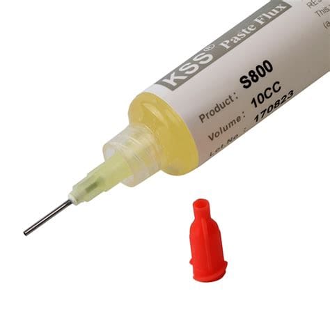
Solder Paste Flux Activity Testing
Solder paste flux activity testing is a method for evaluating the effectiveness of the flux in removing oxides and promoting wetting during the reflow soldering process.
The flux is a chemical compound added to the solder paste to remove oxides and other contaminants from the PCB pads and component leads, and to promote the formation of a metallurgical bond between the solder and the base metals.
Insufficient or excessive flux activity can lead to various soldering defects such as:
- Non-wetting or dewetting of the solder
- Solder balling or beading
- Solder bridging or short circuits
- Flux residue or contamination
Solder paste flux activity can be tested using various methods such as:
- Wetting balance test: This test measures the wetting force and time of a solder pellet or wire on a test coupon coated with the solder paste flux.
- Spread test: This test measures the spread area of a solder ball or paste deposit on a test coupon after reflow, as an indicator of the flux’s ability to promote wetting.
- Surface insulation resistance (SIR) test: This test measures the electrical resistance between adjacent conductors on a test board after exposure to the solder paste flux and reflow, as an indicator of the flux’s corrosivity and ionic contamination.
The acceptable flux activity levels depend on the specific solder paste type, PCB design, and process requirements. In general, a moderate flux activity is preferred to ensure good wetting and minimize flux residue or contamination.
Solder Paste Printing Process Optimization
Solder paste printing process optimization is a method for improving the quality and consistency of the solder paste deposits by adjusting various printing parameters and conditions.
Some of the key factors that can affect the solder paste printing process include:
- Stencil design: The stencil aperture size, shape, and layout should be optimized based on the PCB pad design and solder paste type.
- Printing parameters: The printing speed, pressure, and separation speed should be adjusted based on the solder paste viscosity, stencil thickness, and PCB surface properties.
- Printer setup: The printer alignment, squeegee angle, and stencil-to-PCB gap should be properly set up and calibrated.
- Environmental conditions: The room temperature, humidity, and air flow should be controlled within acceptable ranges to minimize solder paste slump, drying, or contamination.
Solder paste printing process optimization typically involves the following steps:
- Design of experiments (DOE): A systematic approach to varying the printing parameters and measuring their effects on the solder paste deposit quality.
- Statistical analysis: Using statistical tools such as analysis of variance (ANOVA) or regression to identify the most significant factors and their optimal settings.
- Process validation: Verifying the optimized printing parameters on actual production PCBs and monitoring the process capability and stability over time.
- Continuous improvement: Regularly monitoring and adjusting the printing process based on the testing results and feedback from downstream processes such as pick-and-place and reflow soldering.
Frequently Asked Questions (FAQ)
1. What is solder paste, and why is it important in PCB Assembly?
Solder paste is a mixture of powdered solder alloy and flux that is used to establish electrical and mechanical connections between Electronic Components and PCB pads during the reflow soldering process. It is important because it ensures reliable and consistent solder joints that can withstand the stresses and vibrations of the end-use environment.
2. What are the most common defects in solder paste printing, and how can they be prevented?
The most common defects in solder paste printing include insufficient or excessive solder volume, bridging, solder beads, and poor wetting. These defects can be prevented by optimizing the stencil design, printing parameters, and environmental conditions, as well as regularly testing and monitoring the solder paste quality and process capability.
3. What equipment is used for solder paste testing, and how do they work?
Various equipment can be used for solder paste testing, such as solder paste inspection (SPI) systems, automated optical inspection (AOI) systems, 3D profilometers, viscometers, and tackiness testers. These instruments use different techniques such as image analysis, laser scanning, or mechanical measurements to evaluate the solder paste volume, height, area, viscosity, tackiness, and other properties.
4. How often should solder paste testing be performed, and what are the acceptable quality levels?
Solder paste testing should be performed regularly, typically at the beginning of each production shift, after any changes in the printing parameters or materials, and whenever any quality issues are detected downstream. The acceptable quality levels depend on the specific PCB design, component types, and end-use requirements, but generally aim for a solder volume and area within ±20% of the target, a slump of less than 20%, and a tackiness of 0.5 to 2.0 grams.
5. What are some best practices for solder paste printing and testing?
Some best practices for solder paste printing and testing include:
- Using a high-quality solder paste with consistent particle size and flux activity
- Designing the stencil apertures and layout based on the PCB pad geometry and pitch
- Setting up and calibrating the printer alignment, pressure, and speed based on the paste and PCB characteristics
- Controlling the room temperature and humidity within acceptable ranges (typically 20-25°C and 30-50% RH)
- Using SPI or AOI systems to measure the solder paste volume, height, and area after printing
- Performing regular maintenance and cleaning of the stencil, squeegee, and other printer components
- Conducting periodic solder paste testing for viscosity, tackiness, slump, and flux activity
- Analyzing the testing data and trends to identify any process deviations or improvement opportunities
By following these best practices and continuously monitoring and optimizing the solder paste printing process, manufacturers can
No responses yet