Understanding EMI and Its Impact on PCBs
Electromagnetic interference (EMI) is a common issue faced by PCB designers, especially when dealing with power supplies. EMI can cause various problems, such as signal integrity issues, reduced performance, and even complete system failure. In this article, we will explore the sources of power supply EMI, its effects on PCBs, and practical techniques to mitigate these issues.
What is EMI?
EMI is the unintentional generation of electromagnetic energy that can disrupt the proper functioning of electronic devices. It can be caused by various sources, including:
- Switching power supplies
- High-speed digital circuits
- Electrostatic discharge (ESD)
- External electromagnetic fields
EMI can be classified into two main categories:
- Conducted EMI: Interference that propagates through conductive paths, such as power lines, ground planes, and signal traces.
- Radiated EMI: Interference that propagates through the air as electromagnetic waves.
The Impact of EMI on PCBs
EMI can have several negative effects on PCBs, including:
- Signal integrity issues: EMI can cause crosstalk, signal distortion, and noise, leading to compromised data transmission and system performance.
- Reduced component lifespan: Exposure to high levels of EMI can cause premature component failure and reduce the overall reliability of the PCB.
- Compliance issues: Non-compliance with EMC (Electromagnetic Compatibility) regulations can result in costly redesigns, product recalls, and legal consequences.
Sources of Power Supply EMI
Power supplies are one of the primary sources of EMI in PCBs. Switching power supplies, in particular, generate significant amounts of EMI due to their high-frequency switching operation. The main sources of power supply EMI include:
Switching Noise
Switching power supplies operate by rapidly turning on and off power semiconductor devices, such as MOSFETs or IGBTs. This switching action generates high-frequency noise that can propagate through the power lines and couple onto nearby signal traces.
Harmonics
The non-linear nature of switching power supplies results in the generation of harmonic frequencies. These harmonics can cause EMI issues at frequencies much higher than the fundamental switching frequency.
Ringing
Ringing occurs when the parasitic inductance and capacitance of the power supply components form a resonant circuit. This can lead to high-frequency oscillations and EMI.
Common-Mode Noise
Common-mode noise is a type of EMI that occurs when noise currents flow in the same direction through both the power and ground conductors. This noise can be particularly problematic, as it can easily couple onto nearby signal traces.
EMI Mitigation Techniques for PCBs
To combat power supply EMI on your PCB, several techniques can be employed. These techniques can be divided into two main categories: passive and active EMI reduction methods.
Passive EMI Reduction Techniques
Passive EMI reduction techniques involve the use of components and design practices that do not require active control or feedback. Some common passive EMI reduction techniques include:
- Proper Grounding
- Use a solid ground plane to provide a low-impedance return path for high-frequency noise currents.
- Implement a star grounding topology to minimize ground loops and reduce ground bounce.
- Use ground stitching vias to connect ground planes on different layers of the PCB.
- Power and Ground Plane Decoupling
- Place decoupling capacitors close to the power pins of ICs to provide a local, low-impedance path for high-frequency noise currents.
- Use a combination of ceramic and electrolytic capacitors to provide effective decoupling over a wide frequency range.
- Optimize the placement and value of decoupling capacitors based on the frequency response of the power distribution network (PDN).
- Shielding
- Use shielding enclosures or cans to contain EMI generated by sensitive components or circuits.
- Implement proper shielding grounding techniques, such as using multiple ground connections and minimizing the impedance of shield-to-ground connections.
- Consider the use of conductive gaskets or conductive adhesives to ensure proper electrical contact between the shield and the PCB.
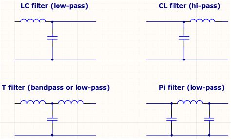
- Filtering
- Use EMI filters, such as ferrite beads or common-mode chokes, to suppress high-frequency noise on power lines and signal traces.
- Implement LC filters to attenuate specific frequency bands of EMI.
- Place filters as close as possible to the noise source to minimize the propagation of EMI.
- Trace Routing and Layout
- Route sensitive signal traces away from noisy power supply circuits and high-speed digital traces.
- Use differential signaling for critical signal paths to reduce the impact of common-mode noise.
- Minimize the loop area of high-frequency current paths to reduce magnetic field coupling.
Active EMI Reduction Techniques
Active EMI reduction techniques involve the use of active components and control systems to mitigate EMI. Some common active EMI reduction techniques include:
- Spread-Spectrum Clocking (SSC)
- Implement SSC to modulate the clock frequency, spreading the energy of the clock harmonics over a wider frequency range.
- Use SSC-capable clock generators or oscillators to reduce the peak amplitude of EMI at specific frequencies.
- Active Filtering
- Employ active filter circuits, such as active EMI filters or active common-mode cancellation circuits, to suppress EMI.
- Use operational amplifiers or other active components to implement high-performance filter topologies.
- Adaptive Noise Cancellation
- Implement adaptive noise cancellation techniques to actively cancel out EMI in real-time.
- Use sensors to detect EMI and generate an out-of-phase signal to cancel the interference.
- Feedback Control Systems
- Implement feedback control systems to monitor and adjust power supply parameters to minimize EMI.
- Use voltage and current sensing to detect EMI and adjust switching frequency, duty cycle, or other parameters to reduce interference.

PCB Layout Considerations for EMI Reduction
Proper PCB layout is crucial for minimizing power supply EMI. Some key layout considerations include:
- Component Placement
- Place noisy components, such as switching power supplies, away from sensitive analog or high-speed digital circuits.
- Group components with similar noise characteristics together to minimize the spread of EMI across the PCB.
- Power and Ground Plane Design
- Use solid power and ground planes to provide a low-impedance return path for high-frequency noise currents.
- Implement power and ground plane segmentation to isolate noisy circuits from sensitive circuits.
- Use guard rings or moats to contain EMI within specific regions of the PCB.
- Trace Routing
- Route power traces as far away as possible from sensitive signal traces to minimize coupling.
- Use trace shielding techniques, such as coplanar shielding or micro-strip shielding, to reduce the coupling of EMI onto signal traces.
- Minimize the length of high-frequency signal traces to reduce the antenna effect and radiated EMI.
- Layer Stackup
- Use a multi-layer PCB stackup to provide dedicated power and ground planes for effective EMI containment.
- Place sensitive signal layers between power and ground planes to provide shielding and reduce the impact of EMI.
- Use high-speed material, such as low-loss dielectrics, to minimize the propagation of EMI through the PCB.
EMI Simulation and Analysis
EMI simulation and analysis tools can be valuable in identifying and mitigating power supply EMI issues during the PCB design phase. Some common EMI simulation and analysis techniques include:
- Power Integrity Analysis
- Use power integrity simulation tools to analyze the impedance profile of the power distribution network (PDN).
- Identify resonances and high-impedance regions that can contribute to EMI issues.
- Optimize the placement and value of decoupling capacitors based on the PDN impedance profile.
- EMI Scanning
- Use near-field probes or EMI scanners to measure the EMI emitted by the PCB during operation.
- Identify hot spots or areas of high EMI intensity and correlate them with specific components or circuits.
- Use the EMI scanning results to guide layout changes and component placement optimization.
- Full-Wave 3D EM Simulation
- Perform full-wave 3D electromagnetic simulations to predict the EMI performance of the PCB.
- Analyze the radiated and conducted EMI emissions from the PCB and identify potential issues.
- Optimize the PCB layout and component placement based on the simulation results to minimize EMI.
EMI Testing and Compliance
To ensure that your PCB meets EMC regulations and standards, EMI testing and compliance validation are essential. Some key aspects of EMI testing and compliance include:
- Pre-Compliance Testing
- Perform in-house pre-compliance testing to identify and address EMI issues before formal compliance testing.
- Use EMI measurement equipment, such as spectrum analyzers and EMI receivers, to measure the EMI emissions from the PCB.
- Follow the relevant EMC standards and test procedures to ensure accurate and reproducible results.
- Formal Compliance Testing
- Engage with certified EMC testing laboratories to perform formal compliance testing.
- Ensure that the PCB meets the applicable EMC standards and regulations, such as FCC Part 15, CISPR, or MIL-STD-461.
- Obtain the necessary certifications and approvals to demonstrate compliance and enable product commercialization.
- Documentation and Reporting
- Maintain comprehensive documentation of the EMI testing and compliance process.
- Generate test reports, including detailed test setups, measurement results, and compliance statements.
- Use the documentation to support product certification, troubleshooting, and future design improvements.
Frequently Asked Questions (FAQ)
- What is the difference between conducted and radiated EMI?
Conducted EMI propagates through conductive paths, such as power lines and signal traces, while radiated EMI propagates through the air as electromagnetic waves. - How can I identify EMI issues on my PCB?
EMI issues can be identified through various methods, including EMI scanning, near-field probing, and spectrum analyzer measurements. These techniques help localize the sources of EMI and guide mitigation efforts. - What are the most effective techniques for reducing power supply EMI?
The most effective techniques for reducing power supply EMI include proper grounding, power and ground plane decoupling, shielding, filtering, and optimized PCB layout. A combination of these techniques is often necessary to achieve the desired EMI reduction. - How important is pre-compliance EMI testing?
Pre-compliance EMI testing is crucial for identifying and addressing EMI issues early in the design process. It helps minimize the risk of failing formal compliance testing and reduces the overall development time and cost. - What are the consequences of non-compliance with EMC regulations?
Non-compliance with EMC regulations can result in product certification delays, costly redesigns, product recalls, and legal consequences. It is essential to ensure that your PCB meets the applicable EMC standards to avoid these issues.
Conclusion
Combating power supply EMI on your PCB requires a comprehensive approach that involves proper design techniques, layout considerations, simulation, and testing. By understanding the sources and impact of EMI, implementing effective mitigation strategies, and following best practices for PCB layout and compliance testing, you can minimize the risk of EMI issues and ensure the reliable operation of your electronic devices.
Remember, EMI reduction is an iterative process that requires continuous refinement and optimization. By staying up-to-date with the latest EMI reduction techniques and tools, and collaborating with experienced EMC engineers, you can effectively combat power supply EMI and develop high-performance, EMC-compliant PCBs.
| EMI Reduction Technique | Description |
|---|---|
| Proper Grounding | Use solid ground planes and star grounding topology |
| Decoupling | Place decoupling capacitors close to IC power pins |
| Shielding | Use shielding enclosures and proper grounding techniques |
| Filtering | Implement EMI filters, such as ferrite beads or LC filters |
| Trace Routing | Route sensitive traces away from noisy circuits |
| Active Filtering | Employ active filter circuits to suppress EMI |
| Spread-Spectrum Clocking | Modulate clock frequency to reduce peak EMI amplitudes |
By implementing these EMI reduction techniques and following best practices for PCB layout and design, you can effectively combat power supply EMI and ensure the reliable operation of your electronic devices.
No responses yet