What is a PCB Solder Mask?
A PCB solder mask, also known as a solder resist or solder stop mask, is a thin lacquer-like layer of polymer applied to the copper traces of a printed circuit board (PCB). Its primary purpose is to prevent solder from bridging between conductors, thereby preventing short circuits. The solder mask also protects the copper from oxidation and contamination, while providing a more aesthetically pleasing appearance to the PCB.
Functions of a PCB Solder Mask
- Prevents solder bridges and short circuits
- Protects copper traces from oxidation and contamination
- Improves the aesthetic appearance of the PCB
- Provides insulation between conductive parts
- Enhances the durability of the PCB
Types of PCB Solder Masks
There are two main types of solder masks used in PCB manufacturing:
- Liquid Photoimageable Solder Mask (LPSM)
- Dry Film Photoimageable Solder Mask (DFSM)
Liquid Photoimageable Solder Mask (LPSM)
LPSM is a liquid-based solder mask that is applied to the PCB using a screen printing or spraying process. After application, the mask is exposed to UV light through a photographic film, which hardens the exposed areas. The unexposed areas are then removed using a developer solution, leaving the desired solder mask pattern on the PCB.
Advantages of LPSM:
– Provides a thinner and more uniform coating
– Offers better resolution and finer pitch capabilities
– Allows for easier repairs and touch-ups
– More cost-effective for smaller production runs
Disadvantages of LPSM:
– Requires a longer processing time
– May have a slightly uneven surface finish
– Can be more prone to pinholes and other defects
Dry Film Photoimageable Solder Mask (DFSM)
DFSM is a dry film that is laminated onto the PCB surface using heat and pressure. The film is then exposed to UV light through a photographic film, which polymerizes the exposed areas. The unexposed areas are removed using a developer solution, leaving the desired solder mask pattern on the PCB.
Advantages of DFSM:
– Provides a more consistent and even surface finish
– Offers better chemical and abrasion resistance
– Faster processing time compared to LPSM
– More suitable for high-volume production
Disadvantages of DFSM:
– Thicker coating compared to LPSM
– May have limitations on fine pitch designs
– More difficult to repair or touch-up
– Higher material costs
Factors to Consider When Choosing a PCB Solder Mask
When selecting the appropriate solder mask for your PCB, consider the following factors:
- Application requirements
- Manufacturing process compatibility
- Material properties
- Cost and production volume
Application Requirements
- Minimum solder mask thickness
- Electrical insulation properties
- Chemical and environmental resistance
- Thermal shock resistance
- Flexibility and adhesion
Manufacturing Process Compatibility
- Screen printing or spraying capabilities for LPSM
- Lamination equipment for DFSM
- UV exposure and developing processes
- Curing and post-curing requirements
Material Properties
- Dielectric strength
- Flammability rating
- Coefficient of thermal expansion (CTE)
- Moisture absorption
- Shelf life and storage conditions
Cost and Production Volume
- Material cost per unit area
- Processing time and labor costs
- Equipment and tooling costs
- Minimum order quantities (MOQs)
- Production volume and scalability

Common PCB Solder Mask Colors
Solder masks are available in a variety of colors, with green being the most common. Other popular colors include:
- Blue
- Red
- Yellow
- Black
- White
- Clear (matte or glossy)
The choice of color is primarily driven by aesthetic preferences, but it can also serve functional purposes such as:
- Improving contrast for component placement and inspection
- Enhancing the visibility of silkscreen markings
- Providing a unique brand identity
Some specialized applications may require specific colors, such as white solder mask for LED lighting or black solder mask for high-end audio equipment.
Solder Mask Application and Curing Process
The application and curing process for solder masks varies depending on the type of mask and the manufacturing process used. However, the general steps involved are as follows:
-
Surface preparation: The PCB surface is cleaned and treated to ensure proper adhesion of the solder mask.
-
Solder mask application: The solder mask is applied to the PCB surface using screen printing, spraying, or lamination, depending on the type of mask used.
-
UV exposure: The applied solder mask is exposed to UV light through a photographic film or direct imaging process, which polymerizes the exposed areas.
-
Developing: The unexposed areas of the solder mask are removed using a developer solution, leaving the desired solder mask pattern on the PCB.
-
Curing: The solder mask is cured using heat or UV light to fully polymerize the material and achieve its final properties.
-
Inspection and testing: The PCB is inspected for defects and tested to ensure compliance with the specified requirements.
Solder Mask Design Considerations
When designing a PCB with a solder mask, consider the following:
-
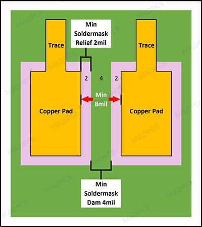
Solder mask clearance: Ensure adequate clearance between the solder mask and the copper features to prevent solder bridging and short circuits.
-
Solder mask expansion: Account for the expansion of the solder mask during the curing process, which can impact the final dimensions of the PCB features.
-
Solder mask registration: Ensure proper alignment between the solder mask and the copper features to maintain the integrity of the PCB design.
-
Solder mask thickness: Specify the appropriate solder mask thickness based on the application requirements and the manufacturing process capabilities.
-
Solder mask color: Select the appropriate solder mask color based on aesthetic preferences and functional requirements.
Troubleshooting Common Solder Mask Issues
Some common issues that may arise with solder masks include:
-
Pinholes: Small holes in the solder mask that can expose the underlying copper and lead to short circuits or corrosion. Pinholes can be caused by contamination, improper curing, or damage during handling.
-
Delamination: Separation of the solder mask from the PCB surface, which can expose the copper and compromise the insulation properties. Delamination can be caused by poor surface preparation, incompatible materials, or excessive stress during assembly or use.
-
Solder mask cracking: Cracks in the solder mask that can expose the underlying copper and lead to reliability issues. Cracking can be caused by excessive stress, thermal cycling, or improper curing.
-
Discoloration: Changes in the color of the solder mask over time due to exposure to UV light, high temperatures, or chemical agents. Discoloration can be aesthetic or indicate a degradation of the material properties.
To minimize these issues, ensure proper surface preparation, material selection, and process control during PCB manufacturing. Regular inspection and testing can also help identify and address any issues early in the production process.
FAQ
-
What is the purpose of a solder mask on a PCB?
A: The primary purposes of a solder mask are to prevent solder bridging and short circuits, protect the copper traces from oxidation and contamination, and provide electrical insulation between conductive parts. -
What are the two main types of solder masks used in PCB manufacturing?
A: The two main types of solder masks are Liquid Photoimageable Solder Mask (LPSM) and Dry Film Photoimageable Solder Mask (DFSM). -
What factors should be considered when choosing a solder mask for a PCB?
A: When choosing a solder mask, consider the application requirements, manufacturing process compatibility, material properties, and cost and production volume. -
Why is green the most common color for PCB solder masks?
A: Green is the most common color for PCB solder masks primarily due to historical reasons and industry standardization. However, other colors are available and may be chosen for aesthetic or functional purposes. -
What are some common issues that can arise with solder masks, and how can they be minimized?
A: Common issues with solder masks include pinholes, delamination, cracking, and discoloration. These issues can be minimized by ensuring proper surface preparation, material selection, process control, and regular inspection and testing during PCB manufacturing.
No responses yet