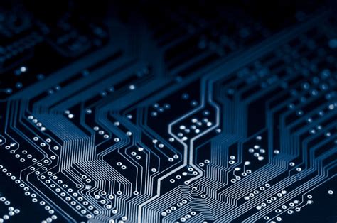
Introduction to PCB Migration
PCB migration is the process of transferring all the components, circuits, and functionality from an existing printed circuit board (PCB) to a new one. This process is often necessary when upgrading to a newer technology, optimizing the design, or replacing a damaged PCB. In this article, we will discuss the steps involved in successfully migrating to a new PCB, along with some best practices and common challenges.
Why Migrate to a New PCB?
There are several reasons why you might need to migrate to a new PCB:
-
Obsolescence: As technology advances, certain components or manufacturing techniques may become obsolete, requiring an update to the PCB design.
-
Performance improvement: A new PCB design may offer better performance, such as faster signal processing, lower power consumption, or improved reliability.
-
Cost reduction: Migrating to a new PCB may allow for cost savings through the use of newer, more affordable components or streamlined manufacturing processes.
-
Size reduction: Advancements in miniaturization techniques may enable a more compact PCB design, which can be crucial for space-constrained applications.
-
Damage or wear: If an existing PCB has suffered damage or wear, migrating to a new PCB may be more cost-effective than attempting repairs.
The PCB Migration Process
The PCB migration process typically involves the following steps:
1. Schematic Review and Update
The first step in PCB migration is to review the existing schematic and update it as necessary. This may involve:
- Replacing obsolete components with their modern equivalents
- Optimizing the circuit design for improved performance or power efficiency
- Adding new features or functionality
2. PCB Layout Design
Once the schematic is updated, the next step is to design the new PCB layout. This involves:
- Choosing the appropriate PCB size and shape
- Placing components and routing traces in an optimal configuration
- Ensuring proper signal integrity and power distribution
- Adhering to manufacturing constraints and design rules
3. Bill of Materials (BOM) Creation
A bill of materials (BOM) is a comprehensive list of all the components required to manufacture the new PCB. Creating an accurate BOM is crucial for ensuring that all necessary components are ordered and available for assembly.
4. Prototype Fabrication and Testing
Before mass production, it is essential to fabricate and test a prototype of the new PCB. This allows for:
- Verifying the functionality and performance of the new design
- Identifying and resolving any issues or defects
- Refining the design based on testing results
5. Manufacturing and Assembly
Once the prototype has been successfully tested and any necessary revisions have been made, the new PCB can be manufactured and assembled. This typically involves:
- Sending the PCB design files to a manufacturing facility
- Procuring the necessary components from suppliers
- Assembling the components onto the PCB using automated or manual processes
- Performing quality control checks to ensure the assembled PCBs meet specifications

Best Practices for PCB Migration
To ensure a successful PCB migration, consider the following best practices:
-
Thorough documentation: Maintain detailed documentation of the existing PCB design, including schematics, layouts, and component specifications. This will facilitate a smoother migration process and serve as a valuable reference.
-
Collaboration with stakeholders: Involve all relevant stakeholders, such as design engineers, component suppliers, and manufacturing partners, early in the migration process. This ensures that all requirements and constraints are considered and helps avoid potential issues down the line.
-
Design for manufacturability (DFM): When designing the new PCB, adhere to DFM principles to ensure that the board can be efficiently and reliably manufactured. This includes considering factors such as component placement, trace routing, and design rule compliance.
-
Thorough testing: Allocate sufficient time and resources for rigorous testing of the new PCB design. This should include functional testing, environmental testing (e.g., temperature, humidity), and reliability testing to ensure the board meets all performance and durability requirements.
-
Version control: Implement a robust version control system to track changes and revisions throughout the migration process. This helps maintain a clear record of the design evolution and facilitates collaboration among team members.
Common Challenges in PCB Migration
PCB migration can present several challenges, including:
-
Component obsolescence: As mentioned earlier, some components used in the existing PCB may be obsolete or no longer available. Identifying suitable replacements that meet the required specifications and sourcing them can be time-consuming and costly.
-
Design complexity: Migrating a complex PCB design with numerous components, high-speed signals, or intricate routing can be challenging. It requires careful planning, simulation, and optimization to ensure the new design meets all performance requirements.
-
Compatibility issues: When migrating to a new PCB, it is crucial to ensure compatibility with existing software, firmware, and mechanical interfaces. Any incompatibilities can lead to significant rework and delays.
-
Manufacturing constraints: The new PCB design must adhere to the manufacturing capabilities and constraints of the chosen fabrication facility. Failing to consider these constraints can result in manufacturability issues and increased costs.
-
Time and cost pressures: PCB migration projects often face tight deadlines and budgetary constraints. Balancing the need for a thorough and reliable migration process with these pressures can be challenging and may require careful project management and prioritization.
PCB Migration Tools and Resources
Several tools and resources are available to support the PCB migration process:
| Tool/Resource | Description |
|---|---|
| PCB design software | Software tools such as Altium Designer, KiCad, or Eagle can be used to create and update PCB schematics and layouts. These tools often include features to help optimize designs for manufacturability and performance. |
| Component databases | Online databases such as Octopart or Mouser can be used to search for and compare components, helping to identify suitable replacements for obsolete parts. |
| Manufacturing partners | Partnering with experienced PCB manufacturing facilities can provide valuable guidance and support throughout the migration process, from design review to final assembly. |
| Industry standards and guidelines | Adhering to industry standards and guidelines, such as those published by IPC (Association Connecting Electronics Industries), can help ensure the new PCB design meets quality and reliability requirements. |
| Online communities and forums | Engaging with online communities and forums focused on PCB design and manufacturing can provide access to a wealth of knowledge and experience from professionals in the field. |
Frequently Asked Questions (FAQ)
-
How long does a typical PCB migration project take?
The duration of a PCB migration project can vary widely depending on the complexity of the design, the availability of components, and the manufacturing process. Simple migrations may take a few weeks, while more complex projects can span several months. Thorough planning and communication with all stakeholders can help streamline the process and minimize delays. -
How much does PCB migration cost?
The cost of PCB migration depends on factors such as the size and complexity of the board, the components required, and the manufacturing process. It is essential to consider not only the direct costs of design, components, and fabrication but also indirect costs such as testing, rework, and potential delays. Careful budgeting and cost management throughout the project can help keep expenses under control. -
Can I migrate just a portion of an existing PCB design?
Yes, it is possible to migrate a portion of an existing PCB design while leaving other parts unchanged. This can be useful when upgrading specific components or adding new features without redesigning the entire board. However, it is important to ensure that any changes are compatible with the existing design and do not introduce new issues or constraints. -
How do I ensure the new PCB meets all regulatory requirements?
To ensure the new PCB meets all regulatory requirements, such as electromagnetic compatibility (EMC) or safety standards, it is important to consider these requirements from the outset of the design process. This may involve conducting simulations, testing, and obtaining necessary certifications. Working with experienced manufacturing partners and staying up-to-date with the latest industry standards can help ensure compliance. -
What should I do if I encounter issues during the PCB migration process?
If issues arise during the PCB migration process, it is important to address them promptly and systematically. This may involve: - Clearly defining the problem and its impact
- Collaborating with relevant stakeholders to identify potential solutions
- Conducting additional testing or simulations to validate proposed changes
- Documenting any modifications and updating project plans accordingly
Open communication and a proactive approach to problem-solving can help minimize the impact of issues and keep the migration project on track.
Conclusion
PCB migration is a complex process that requires careful planning, execution, and collaboration among various stakeholders. By understanding the reasons for migration, following best practices, and being aware of common challenges, you can increase the likelihood of a successful project outcome. Leveraging available tools and resources, such as PCB design software, component databases, and manufacturing partners, can further streamline the migration process and ensure the new PCB meets all performance, reliability, and regulatory requirements.
No responses yet