
Introduction to PCB current capacity
When designing a printed circuit board (PCB), one of the crucial aspects to consider is the current carrying capacity of the power planes. The power planes are responsible for distributing power throughout the PCB, and ensuring that they can handle the required current is essential for the proper functioning and reliability of the electronic device. In this article, we will delve into the methods and factors involved in calculating the current capacity of PCB power planes.
Understanding Current Density
What is Current Density?
Current density is a measure of the amount of electric current flowing through a unit area of a conductor. It is expressed in units of amperes per square meter (A/m²) or amperes per square millimeter (A/mm²). Understanding current density is fundamental to determining the current carrying capacity of PCB power planes.
Factors Affecting Current Density
Several factors influence the current density in PCB power planes:
-
Conductor material: The conductivity of the material used for the power planes affects the current density. Copper is the most common choice due to its high conductivity.
-
Thickness of the power plane: Thicker power planes can carry more current than thinner ones, as they have a larger cross-sectional area.
-
Temperature: As the temperature of the PCB increases, the resistance of the conductors also increases, leading to a reduction in current carrying capacity.
-
Ambient temperature: The surrounding temperature also impacts the current carrying capacity of the power planes, as it affects the heat dissipation capabilities of the PCB.
Calculating Current Capacity
IPC-2152 Standard
The IPC-2152 standard, titled “Standard for Determining Current-Carrying Capacity in Printed Board Design,” provides guidelines for calculating the current capacity of PCB traces and power planes. This standard takes into account various factors, such as conductor material, thickness, temperature rise, and ambient temperature.
Calculation Methods
There are two primary methods for calculating the current capacity of PCB power planes:
-
Analytical method: This method involves using mathematical equations and formulas to determine the current capacity based on the physical properties of the power planes, such as conductor material, thickness, and width.
-
Simulation method: This approach utilizes specialized software tools to simulate the current flow and heat distribution in the PCB power planes. Simulation allows for more accurate results, as it can take into account complex geometries and thermal effects.
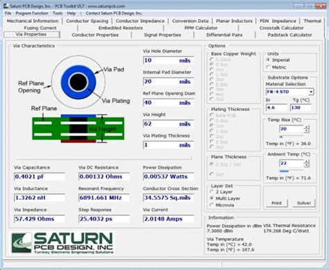
Analytical Method Example
To illustrate the analytical method, let’s consider a simple example. Suppose we have a copper power plane with a thickness of 1 oz/ft² (35 µm) and a width of 10 mm. We want to determine the maximum current the power plane can carry without exceeding a temperature rise of 10°C above the ambient temperature.
Using the IPC-2152 standard, we can refer to the provided tables to find the current carrying capacity for a 1 oz/ft² copper conductor with a width of 10 mm and a temperature rise of 10°C. From the table, we find that the maximum current is approximately 5.8 A.
| Copper Thickness | Conductor Width | Temperature Rise | Current Capacity |
|---|---|---|---|
| 1 oz/ft² | 10 mm | 10°C | 5.8 A |
Simulation Method Example
For a more accurate and comprehensive analysis, the simulation method is preferred. Specialized PCB design software, such as Altium Designer or Cadence OrCAD, offers built-in tools for simulating current flow and heat distribution in power planes.
These tools allow designers to define the PCB stackup, specify the power plane geometries, and set the desired operating conditions. The software then performs a detailed simulation, considering factors such as conductor material, thickness, ambient temperature, and heat dissipation.
The simulation results provide a visual representation of the current density distribution and temperature gradients across the power planes. Designers can use this information to identify hotspots, optimize the power plane layout, and ensure that the current carrying capacity is sufficient for the intended application.

Design Considerations
Power Plane Thickness
One of the key design considerations when determining the current capacity of PCB power planes is the thickness of the copper layer. Thicker power planes can carry more current, as they have a larger cross-sectional area. However, increasing the thickness also adds to the overall cost and weight of the PCB.
Common copper thicknesses used in PCBs include:
- 0.5 oz/ft² (17.5 µm)
- 1 oz/ft² (35 µm)
- 2 oz/ft² (70 µm)
- 3 oz/ft² (105 µm)
When selecting the appropriate thickness, designers must balance the current carrying requirements with the cost and manufacturing constraints of the PCB.
Power Plane Geometry
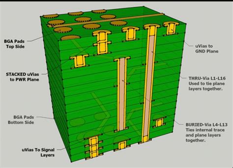
The geometry of the power planes also plays a role in determining the current capacity. Wide, uninterrupted power planes offer lower resistance and better current carrying capacity compared to narrow or segmented planes.
Designers should strive to create power planes with minimal interruptions and avoid placing large numbers of vias or holes in the power planes, as they can impede current flow and create localized hotspots.
Thermal Management
Proper thermal management is crucial for maintaining the current carrying capacity of PCB power planes. As the temperature of the PCB increases, the resistance of the conductors also increases, leading to a reduction in current capacity.
To mitigate this issue, designers can employ various thermal management techniques:
- Using thermal vias to transfer heat from the power planes to other layers or heatsinks.
- Incorporating copper pours or heat spreaders to distribute heat more evenly across the PCB.
- Selecting PCB materials with higher thermal conductivity, such as metal-core PCBs or insulated metal substrates (IMS).
By implementing effective thermal management strategies, designers can ensure that the PCB power planes can operate at their maximum current carrying capacity without excessive temperature rise.
Frequently Asked Questions (FAQ)
-
What is the difference between current density and current capacity?
Current density refers to the amount of electric current flowing through a unit area of a conductor, expressed in A/m² or A/mm². Current capacity, on the other hand, is the maximum amount of current a conductor can carry without exceeding a specified temperature rise. -
How does the ambient temperature affect the current carrying capacity of PCB power planes?
The ambient temperature plays a significant role in determining the current carrying capacity of PCB power planes. As the ambient temperature increases, the ability of the PCB to dissipate heat decreases, leading to a reduction in current capacity. Designers must consider the expected operating environment and specify the maximum ambient temperature when calculating the current capacity. -
Can I use different copper thicknesses for different layers in a PCB?
Yes, it is common practice to use different copper thicknesses for different layers in a PCB. For example, the power planes may have a thicker copper layer to handle higher currents, while signal layers may use thinner copper to achieve finer trace widths and spacing. However, it is essential to consider the manufacturing capabilities and costs associated with using multiple copper thicknesses. -
What are the consequences of exceeding the current carrying capacity of PCB power planes?
Exceeding the current carrying capacity of PCB power planes can lead to several issues, including: - Excessive temperature rise, which can cause component failure or degradation.
- Voltage drop across the power planes, leading to reduced performance or malfunction of connected devices.
- Increased risk of thermal runaway, where the temperature continues to rise uncontrollably.
-
Potential damage to the PCB, such as delamination or conductor failure.
-
How can I verify the current carrying capacity of my PCB power planes?
To verify the current carrying capacity of PCB power planes, designers can use a combination of analytical calculations and simulation tools. The IPC-2152 standard provides guidelines and tables for estimating the current capacity based on conductor material, thickness, and temperature rise. Additionally, PCB design software with built-in simulation capabilities can provide more accurate and comprehensive analysis, considering factors such as power plane geometry, thermal effects, and ambient conditions. It is also recommended to perform physical testing and measurements on prototype boards to validate the current carrying capacity under real-world conditions.
Conclusion
Calculating the current carrying capacity of PCB power planes is a critical aspect of electronic design. By understanding the factors that influence current density, such as conductor material, thickness, and temperature, designers can ensure that their PCBs can handle the required currents without compromising performance or reliability.
The IPC-2152 standard provides guidelines and methods for calculating the current capacity, including analytical equations and tables. However, for more accurate and comprehensive analysis, simulation tools offered by PCB design software are invaluable.
Designers must also consider factors such as power plane thickness, geometry, and thermal management when optimizing the current carrying capacity of their PCBs. By following best practices and leveraging the available tools and standards, designers can create robust and reliable PCBs that meet the power distribution requirements of their electronic devices.
No responses yet