
What are Antipads and Why Do They Matter for Signal Integrity?
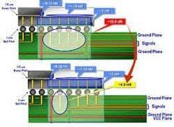
Antipads, also known as clearance holes or relief holes, are an essential feature in multilayer printed circuit boards (PCBs). They are the ring-shaped spaces surrounding vias and through-holes that electrically isolate the via from the surrounding copper planes on the inner layers of the PCB. Antipads play a crucial role in maintaining signal integrity by preventing unwanted coupling and crosstalk between signals traveling through vias and the power or ground planes.
In high-speed digital designs, signal integrity is of utmost importance. As signal frequencies increase and rise times decrease, the impact of parasitic effects like crosstalk, reflections, and electromagnetic interference (EMI) become more pronounced. These effects can lead to signal distortion, jitter, and even complete signal failure, compromising the performance and reliability of the electronic device.
Antipads help mitigate these issues by providing a controlled impedance environment for signals transitioning through the PCB’s layers. By adjusting the size and shape of antipads, designers can fine-tune the impedance of vias and optimize signal integrity.
Key Aspects of Antipads That Affect Signal Integrity
-
Size: The size of the antipad directly influences the impedance of the via. Larger antipads result in higher impedance, while smaller antipads lead to lower impedance.
-
Shape: Antipads are typically circular, but other shapes like squares or ovals can be used to optimize impedance matching and reduce EMI.
-
Placement: The location of antipads relative to the signal traces and other components can impact crosstalk and signal reflections.
Calculating Antipad Size for Optimal Impedance Control
To ensure optimal signal integrity, it is crucial to calculate the appropriate antipad size for a given via geometry and PCB stackup. The goal is to match the impedance of the via to the characteristic impedance of the signal traces, typically 50Ω or 100Ω in high-speed digital designs.
The impedance of a via is determined by its geometry, the dielectric constant of the PCB material, and the size of the antipad. The following equation can be used to estimate the impedance of a via:
Z₀ = 60 × ln(D/d) ÷ √ε_r
Where:
– Z₀ is the characteristic impedance of the via (in Ω)
– D is the diameter of the antipad (in mils)
– d is the diameter of the via drill hole (in mils)
– ε_r is the dielectric constant of the PCB material
For example, consider a via with a drill hole diameter of 10 mils in a PCB with a dielectric constant of 4.0. To achieve a target impedance of 50Ω, we can calculate the required antipad diameter:
D = d × e^((Z₀ × √ε_r) ÷ 60)
= 10 × e^((50 × √4.0) ÷ 60)
≈ 22.14 mils
Therefore, an antipad diameter of approximately 22 mils would be needed to achieve a 50Ω impedance for this via.
Antipad Size vs. Impedance Table
| Via Drill Diameter (mils) | Antipad Diameter (mils) | PCB Dielectric Constant | Resulting Impedance (Ω) |
|---|---|---|---|
| 10 | 20 | 4.0 | 41.6 |
| 10 | 22 | 4.0 | 49.9 |
| 10 | 24 | 4.0 | 57.6 |
| 8 | 18 | 4.5 | 44.3 |
| 8 | 20 | 4.5 | 53.1 |
| 8 | 22 | 4.5 | 61.3 |
The Impact of Antipad Shape on Signal Integrity
While circular antipads are the most common, other shapes can be used to optimize signal integrity and EMI performance. The choice of antipad shape depends on factors such as the via geometry, signal frequency, and routing constraints.
Circular Antipads
Circular antipads are the default choice for most PCB designs. They provide a symmetrical and predictable impedance environment for signals passing through vias. Circular antipads are easy to manufacture and do not require any special considerations during PCB layout.
However, in certain situations, circular antipads may not provide the best signal integrity performance. For example, when vias are located close to the edges of signal traces, the circular antipad may not provide sufficient clearance, leading to increased crosstalk and reflections.
Square Antipads
Square antipads offer several advantages over circular antipads in specific scenarios. They provide more clearance between the via and the surrounding copper plane, reducing the risk of crosstalk and reflections when vias are placed near signal traces.
Square antipads also have a smaller area compared to circular antipads of the same dimensions, which can help reduce the overall capacitance of the via. This is particularly beneficial in high-frequency designs where minimizing parasitic capacitance is critical for maintaining signal integrity.
However, square antipads can be more challenging to manufacture consistently, especially for smaller via sizes. They may also require more precise alignment during the PCB layout process to ensure proper clearance and impedance control.
Oval Antipads
Oval antipads are a compromise between circular and square antipads. They provide the benefits of increased clearance and reduced capacitance like square antipads while being easier to manufacture and align during PCB layout.
Oval antipads are particularly useful when vias are placed in a staggered pattern or when there are space constraints that prevent the use of larger circular antipads. By orienting the oval antipads along the direction of the signal traces, designers can minimize crosstalk and reflections while maintaining a compact layout.

Placement Strategies for Antipads
The placement of antipads relative to signal traces and other components can have a significant impact on signal integrity. Poor placement can lead to increased crosstalk, reflections, and EMI, while optimal placement can help minimize these issues and improve overall system performance.
Antipad Placement Guidelines
-
Avoid placing vias too close to the edges of signal traces. This can cause unwanted coupling and reflections, degrading signal integrity. Maintain a minimum clearance between vias and traces based on the PCB manufacturing capabilities and signal requirements.
-
Stagger vias when routing multiple signals through the same area of the PCB. Staggered via placement helps reduce crosstalk by increasing the distance between adjacent vias and minimizing the overlap of antipads.
-
Use ground vias strategically to provide shielding and reduce crosstalk between signal vias. Place ground vias adjacent to signal vias, especially for high-speed or sensitive signals, to create a barrier against electromagnetic interference.
-
Consider the impact of antipad placement on power integrity. Avoid placing vias with large antipads near power pins or planes, as this can create discontinuities in the power distribution network and lead to increased impedance and noise.
-
Optimize antipad placement for differential pairs. Ensure that the antipads for differential vias are symmetrical and have consistent spacing to maintain differential signal integrity and minimize mode conversion.
Example of Staggered Via Placement
     Signal Via    Ground Via
         ●             ●
           ●             ●
         ●             ●
           ●             ●
By staggering the signal and ground vias, designers can reduce crosstalk and improve signal integrity compared to a straight line placement.
Frequently Asked Questions (FAQ)
1. What is the primary purpose of antipads in multilayer PCBs?
Antipads serve as a means to electrically isolate vias from the surrounding copper planes on the inner layers of a PCB. They help maintain signal integrity by preventing unwanted coupling and crosstalk between signals traveling through vias and the power or ground planes.
2. How does the size of an antipad affect the impedance of a via?
The size of an antipad directly influences the impedance of a via. Larger antipads result in higher impedance, while smaller antipads lead to lower impedance. Designers can adjust the size of antipads to match the impedance of the via to the characteristic impedance of the signal traces, ensuring optimal signal integrity.
3. What are the advantages of using square or oval antipads compared to circular antipads?
Square and oval antipads offer several advantages over circular antipads in certain situations. They provide more clearance between the via and the surrounding copper plane, reducing the risk of crosstalk and reflections when vias are placed near signal traces. Square and oval antipads also have a smaller area compared to circular antipads of the same dimensions, which can help reduce the overall capacitance of the via.
4. How does the placement of antipads impact signal integrity?
The placement of antipads relative to signal traces and other components can significantly impact signal integrity. Poor placement can lead to increased crosstalk, reflections, and EMI, while optimal placement can help minimize these issues. Designers should follow guidelines such as maintaining a minimum clearance between vias and traces, staggering vias when routing multiple signals, using ground vias for shielding, and optimizing antipad placement for differential pairs.
5. What other factors should be considered when designing antipads for high-speed PCBs?
In addition to size, shape, and placement, other factors to consider when designing antipads for high-speed PCBs include:
- Material selection: The dielectric constant and loss tangent of the PCB material influence the impedance and signal attenuation of vias.
- Manufacturing capabilities: The minimum via size, antipad size, and spacing that can be reliably manufactured depend on the PCB fabrication process and tolerances.
- Signal requirements: The bandwidth, rise time, and sensitivity of the signals passing through the vias should be considered when determining the appropriate antipad design.
- Simulation and validation: Signal integrity simulations and measurements should be performed to validate the antipad design and ensure that it meets the required performance criteria.
By carefully considering these factors and following best practices for antipad design, engineers can optimize signal integrity, minimize EMI, and ensure the reliable operation of high-speed digital systems in multilayer PCBs.
No responses yet