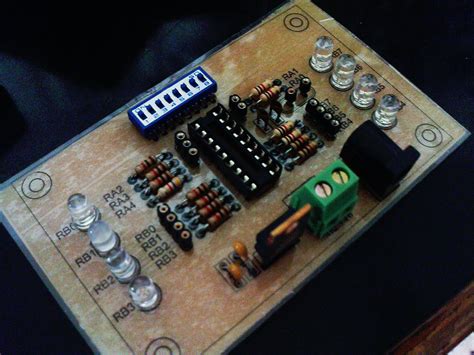
What You’ll Need
Before we begin, gather the following materials and tools:
Toner Transfer Method
- Laser printer
- Glossy photo paper
- Copper clad board
- Clothes iron
- Acetone or nail polish remover
- Ferric chloride solution
- Plastic tray
- Rubber gloves
- Safety goggles
- Drill and bits (for drilling holes)
UV Exposure Method
- UV exposure unit
- Photosensitive copper clad board
- Transparency film
- Inkjet printer
- Developing solution
- Etching solution (ferric chloride or sodium persulfate)
- Plastic tray
- Rubber gloves
- Safety goggles
- Drill and bits (for drilling holes)
Method 1: Toner Transfer
Step 1: Design Your PCB
Using PCB design software (e.g., Eagle, KiCad, or EasyEDA), create your circuit board layout. Ensure that your design is mirrored, as the toner transfer process will flip the image.
Step 2: Print Your Design
Print your mirrored PCB design onto glossy photo paper using a laser printer. Use the highest quality settings for the best results.
Step 3: Prepare the Copper Clad Board
Clean the copper clad board with acetone or nail polish remover to remove any dirt or grease. Cut the board to the desired size, ensuring it’s slightly larger than your printed design.
Step 4: Transfer the Toner
Place the printed design face-down onto the copper clad board. Apply heat using a clothes iron set to its highest temperature without steam. Press firmly and evenly for 5-10 minutes, ensuring the toner adheres to the copper.
Step 5: Remove the Paper
Soak the board in warm water for a few minutes. Gently peel off the paper, revealing the transferred toner on the copper surface. Touch up any imperfections with a permanent marker.
Step 6: Etch the Board
Wearing rubber gloves and safety goggles, submerge the board in a plastic tray filled with ferric chloride solution. Agitate the tray occasionally, and monitor the etching process. Once the exposed copper is completely removed (usually 15-30 minutes), remove the board and rinse it with water.
Step 7: Clean and Drill
Remove the remaining toner using acetone or nail polish remover. Drill any necessary holes for components using a drill and appropriate bits.
Method 2: UV Exposure
Step 1: Design Your PCB
Create your PCB layout using design software, ensuring the design is not mirrored.
Step 2: Print the Transparency
Print your design onto a transparency film using an inkjet printer. Use the highest quality settings and allow the ink to dry completely.
Step 3: Expose the Photosensitive Board
Place the transparency film onto the photosensitive copper clad board, with the printed side facing the photosensitive layer. Secure the transparency using tape. Expose the board to UV light in an exposure unit for the recommended time (usually 2-5 minutes).
Step 4: Develop the Board
Submerge the exposed board in a developing solution, following the manufacturer’s instructions. The unexposed photosensitive layer will dissolve, leaving behind the PCB pattern.
Step 5: Etch the Board
Wearing rubber gloves and safety goggles, place the developed board in a plastic tray filled with etching solution (ferric chloride or sodium persulfate). Agitate the tray occasionally, and monitor the etching process. Once the exposed copper is completely removed (usually 15-30 minutes), remove the board and rinse it with water.
Step 6: Clean and Drill
Remove the remaining photosensitive layer using acetone or as directed by the manufacturer. Drill any necessary holes for components using a drill and appropriate bits.

Tips for Success
- Always work in a well-ventilated area and wear protective gear when handling chemicals.
- Double-check your PCB design for errors before printing.
- Experiment with different exposure times and etching durations to achieve optimal results.
- Use high-quality materials for the best outcome.
- Practice proper disposal of chemical solutions according to local regulations.
Frequently Asked Questions (FAQ)
1. Can I use an inkjet printer for the toner transfer method?
No, the toner transfer method requires a laser printer. Inkjet printers use liquid ink, which will not transfer properly to the copper clad board.
2. How long does it take to etch a PCB?
Etching time varies depending on the size of your board and the strength of the etching solution. On average, it takes 15-30 minutes to etch a PCB.
3. What is the best software for designing PCBs?
There are several popular PCB design software options, including Eagle, KiCad, and EasyEDA. Choose the one that best suits your needs and skill level.
4. Can I reuse the etching solution?
Yes, you can reuse the etching solution multiple times. However, its effectiveness will diminish over time, so you may need to increase the etching duration or replace the solution eventually.
5. How do I dispose of the chemical solutions used in the PCB fabrication process?
Always follow local regulations for the proper disposal of chemical solutions. Contact your local waste management authority for guidance on disposing of ferric chloride and other chemicals used in the process.
Conclusion
Creating your own PCBs at home is a rewarding and educational experience for electronics enthusiasts. By following these step-by-step instructions for the toner transfer and UV exposure methods, you’ll be well on your way to fabricating professional-quality PCBs in the comfort of your own workshop. Remember to prioritize safety, use high-quality materials, and practice patience throughout the process. Happy PCB making!

No responses yet