Introduction to High Speed PCB Layout
High speed PCB layout is a critical aspect of designing modern electronic systems. As signal speeds and frequencies continue to increase, the challenges associated with designing reliable and efficient PCBs become more complex. Proper layout techniques are essential to ensure signal integrity, minimize electromagnetic interference (EMI), and optimize performance.
In this article, we will explore various high speed PCB layout techniques, including signal routing, power distribution, grounding, and more. By understanding and applying these techniques, designers can create robust and reliable high speed PCBs that meet the demanding requirements of today’s electronic systems.
Understanding Signal Integrity in High Speed PCBs
What is Signal Integrity?
Signal integrity refers to the ability of an electrical signal to maintain its intended characteristics as it propagates through a system. In high speed PCBs, signal integrity is a critical concern due to the high frequencies and fast rise times involved. Poor signal integrity can lead to issues such as signal distortion, crosstalk, and EMI, which can degrade system performance and reliability.
Factors Affecting Signal Integrity
Several factors can impact signal integrity in high speed PCBs, including:
- Trace geometry and routing
- Dielectric materials and properties
- Impedance matching and termination
- Crosstalk and electromagnetic coupling
- Power distribution and grounding
By understanding and addressing these factors, designers can minimize signal integrity issues and ensure reliable operation of high speed circuits.
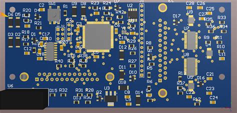
 PCB-layout-Techniques-ca92c159e4ac11eea835f7f8ca593eb4.jpeg” alt=”” class=”wp-image-136″ srcset=”https://electronicmanufacturingservice.org/wp-content/uploads/2024/03/PCB-Layout-Techniques-ca92c159e4ac11eea835f7f8ca593eb4.jpeg”>
High Speed PCB Layout Techniques
Trace Routing and Geometry
Proper trace routing and geometry are essential for maintaining signal integrity in high speed PCBs. Some key considerations include:
- Minimizing trace length to reduce signal propagation delay and attenuation
- Using controlled impedance traces to match the characteristic impedance of the system
- Avoiding sharp bends and corners, which can cause signal reflections and distortion
- Providing adequate spacing between traces to minimize crosstalk and coupling
| Trace Parameter | Recommended Value |
|---|---|
| Trace Width | Depends on impedance requirements and current carrying capacity |
| Trace Spacing | 3-5 times the trace width for minimal crosstalk |
| Trace Corners | Use 45° angles or smooth curves instead of 90° bends |
Power Distribution and Decoupling
Proper power distribution and decoupling are critical for maintaining signal integrity and reducing noise in high speed PCBs. Some key techniques include:
- Using dedicated power and ground planes to provide low-impedance paths for current flow
- Placing decoupling capacitors close to ICs to minimize power supply noise and transients
- Implementing power islands to isolate sensitive circuits from noisy regions of the board
- Using split power planes or ferrite beads to isolate digital and analog power domains
| Decoupling Capacitor Parameter | Recommended Value |
|---|---|
| Capacitance Value | 0.01 μF to 10 μF, depending on frequency and current requirements |
| Placement | As close to the IC power pins as possible |
| Quantity | Sufficient to meet the IC’s transient current demands |
Grounding Strategies
Effective grounding is essential for controlling noise, minimizing EMI, and ensuring signal integrity in high speed PCBs. Some key grounding strategies include:
- Using a solid ground plane to provide a low-impedance return path for signals
- Implementing a star grounding scheme to minimize ground loops and noise coupling
- Providing separate analog and digital ground planes, connected at a single point
- Using stitching vias to connect ground planes on different layers and minimize impedance
| Grounding Parameter | Recommended Value |
|---|---|
| Ground Plane Thickness | Depends on the desired impedance and current carrying capacity |
| Via Spacing | Sufficient to maintain low-impedance ground connections |
| Ground Plane Gaps | Minimize gaps to prevent impedance discontinuities |
EMI Reduction Techniques
Electromagnetic interference (EMI) can be a significant challenge in high speed PCBs, leading to signal integrity issues and regulatory compliance problems. Some key EMI reduction techniques include:
- Proper shielding of sensitive circuits and components
- Using differential signaling to cancel out electromagnetic fields
- Implementing spread-spectrum clocking to reduce peak EMI emissions
- Providing adequate filtering on power supply lines and I/O ports
| EMI Reduction Technique | Description |
|---|---|
| Shielding | Enclosing sensitive circuits in conductive enclosures to attenuate EMI |
| Differential Signaling | Using paired signals with opposite polarity to cancel out electromagnetic fields |
| Spread-Spectrum Clocking | Modulating the clock frequency to spread EMI energy over a wider bandwidth |

Advanced High Speed PCB Layout Techniques
Via Optimization
Vias are essential for connecting traces on different layers of a PCB, but they can also introduce signal integrity issues in high speed designs. Some advanced via optimization techniques include:
- Using blind and buried vias to minimize stub lengths and reduce capacitance
- Implementing via stubs and back-drilling to remove unused portions of the via
- Optimizing via size and placement to minimize impedance discontinuities
| Via Optimization Technique | Description |
|---|---|
| Blind and Buried Vias | Vias that do not extend through the entire board thickness, reducing stub lengths |
| Back-Drilling | Removing unused portions of the via to minimize stub effects |
| Via Size and Placement | Optimizing via dimensions and location to minimize impedance discontinuities |
Signal Integrity Simulation and Analysis
Signal integrity simulation and analysis tools can help designers identify and address potential issues before fabricating the PCB. Some key techniques include:
- Using SPICE-based simulators to model trace impedance and signal propagation
- Performing time-domain reflectometry (TDR) analysis to identify impedance discontinuities
- Conducting frequency-domain analysis to assess the impact of losses and dispersion
| Simulation Technique | Description |
|---|---|
| SPICE Simulation | Modeling trace impedance and signal propagation using circuit simulators |
| TDR Analysis | Measuring reflections to identify impedance discontinuities along a trace |
| Frequency-Domain Analysis | Assessing the impact of losses and dispersion on signal integrity |
Best Practices for High Speed PCB Layout
- Start with a well-defined schematic and component placement
- Use a multi-layer PCB with dedicated power and ground planes
- Route critical signals on inner layers to minimize EMI and crosstalk
- Provide adequate decoupling and filtering for power supplies
- Implement consistent grounding strategies throughout the design
- Simulate and analyze signal integrity early in the design process
- Follow manufacturer guidelines for component placement and routing
- Use high-quality materials and fabrication processes for best results
Frequently Asked Questions (FAQ)
1. What is the most important factor in maintaining signal integrity in high speed PCBs?
Proper trace routing and impedance control are the most critical factors in maintaining signal integrity. Traces should be routed carefully to minimize length, avoid discontinuities, and match the characteristic impedance of the system.
2. How can I minimize crosstalk between adjacent traces?
To minimize crosstalk, ensure adequate spacing between traces (at least 3-5 times the trace width), route critical signals on different layers, and use guard traces or ground planes to provide shielding.
3. What is the purpose of decoupling capacitors, and where should they be placed?
Decoupling capacitors are used to minimize power supply noise and provide a stable voltage reference for ICs. They should be placed as close to the IC power pins as possible to be most effective.
4. How can I reduce EMI in my high speed PCB design?
To reduce EMI, use proper shielding techniques, implement differential signaling, use spread-spectrum clocking, and provide adequate filtering on power supplies and I/O ports.
5. When should I use blind and buried vias in my high speed PCB layout?
Blind and buried vias are useful for minimizing stub lengths and reducing capacitance in high speed designs. They are particularly beneficial when routing dense, high-speed signals on inner layers of the PCB.
Conclusion
High speed PCB layout is a complex and challenging task that requires careful consideration of signal integrity, power distribution, grounding, and EMI. By understanding and applying the techniques discussed in this article, designers can create robust and reliable high speed PCBs that meet the demanding requirements of modern electronic systems.
Proper trace routing, impedance control, decoupling, and grounding are essential for maintaining signal integrity and minimizing noise. Advanced techniques such as via optimization and signal integrity simulation can further improve performance and reliability.
As signal speeds and frequencies continue to increase, the importance of high speed PCB layout techniques will only continue to grow. By staying up-to-date with best practices and emerging technologies, designers can ensure their PCBs are well-equipped to handle the challenges of high speed design.
No responses yet