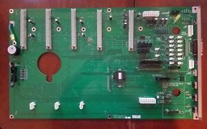
Introduction to Backplane PCB Design
A backplane PCB, also known as a motherboard, is a printed circuit board that serves as the backbone of a computer system or other electronic device. It provides the electrical connections and mechanical support for the various components and modules that make up the system. In high-speed applications, the design and layout of the backplane PCB become critical factors in ensuring reliable performance and signal integrity.
In this article, we will delve into the key aspects of high-speed backplane PCB design and provide valuable tips for optimizing the layout to achieve optimal performance.
Understanding the Challenges of High-Speed Backplane Design
Signal Integrity Issues
One of the primary challenges in high-speed backplane design is maintaining signal integrity. As the operating frequencies of electronic systems continue to increase, the PCB traces and interconnects become more susceptible to various signal integrity issues. These issues can include:
- Crosstalk: Unwanted coupling of signals between adjacent traces.
- Reflections: Signal reflections caused by impedance mismatches.
- Electromagnetic Interference (EMI): Interference from external sources or between different parts of the system.
- Attenuation: Loss of signal strength over long distances.
To mitigate these signal integrity issues, careful consideration must be given to the PCB layout, trace routing, and impedance control.
Power Integrity Concerns
Another critical aspect of high-speed backplane design is power integrity. As the system operates at higher frequencies and consumes more power, the power distribution network (PDN) must be designed to provide a stable and clean power supply to all components. Power integrity issues can manifest as:
- Voltage drops: Excessive voltage drops across the power planes due to high current demand.
- Ground bounce: Voltage fluctuations on the ground plane caused by sudden changes in current.
- Power supply noise: Noise generated by switching activity and propagated through the power distribution network.
Proper design of the power distribution network, including the use of decoupling capacitors and power plane partitioning, is essential to maintain power integrity.
PCB layout tips for High-Speed Backplane Design
Trace Routing and Impedance Control
Proper trace routing and impedance control are crucial for maintaining signal integrity in high-speed backplane PCBs. Here are some tips to consider:
- Use controlled impedance traces: Match the impedance of the traces to the characteristic impedance of the system (typically 50 ohms for single-ended signals and 100 ohms for differential pairs).
- Keep trace lengths short: Minimize the length of traces to reduce signal attenuation and delay.
- Avoid sharp bends: Use smooth curves or 45-degree angles instead of 90-degree bends to minimize reflections.
- Maintain consistent spacing: Ensure consistent spacing between traces and adjacent layers to maintain impedance and reduce crosstalk.
- Use differential signaling: Implement differential signaling for high-speed signals to improve noise immunity and reduce EMI.
| Parameter | Recommended Value |
|---|---|
| Trace Width | Determined by impedance requirements |
| Trace Spacing | 3x trace width (minimum) |
| Differential Pair Spacing | 2x trace width (minimum) |
| Via Hole Size | Determined by current carrying capacity |
Power Distribution Network Design
A well-designed power distribution network is essential for maintaining power integrity in high-speed backplane PCBs. Consider the following tips:
- Use dedicated power planes: Assign dedicated power planes for each voltage level to provide low-impedance power distribution.
- Implement proper decoupling: Place decoupling capacitors close to the power pins of ICs to suppress high-frequency noise and provide local energy storage.
- Partition power planes: Divide the power planes into separate sections for different components or modules to minimize noise coupling.
- Use power plane cutouts: Create cutouts in the power planes around high-speed signals to reduce capacitive coupling and improve signal integrity.
- Minimize power plane impedance: Reduce the impedance of the power planes by using thicker copper and minimizing the distance between the power and ground planes.
| Component | Recommended Placement |
|---|---|
| Decoupling Capacitors | Close to IC power pins |
| Bulk Capacitors | Near power supply input |
| Ferrite Beads | In series with power supply lines |
Signal Routing and Layer Stackup
The layer stackup and signal routing strategy play a significant role in the performance of high-speed backplane PCBs. Consider the following guidelines:
- Use a symmetrical stackup: Implement a symmetrical layer stackup to balance the dielectric constant and minimize warpage.
- Separate signal layers: Route high-speed signals on dedicated layers, separated from power and ground planes, to reduce crosstalk and EMI.
- Use ground planes: Place ground planes adjacent to high-speed signal layers to provide shielding and reduce cross-talk.
- Minimize via usage: Reduce the number of vias in high-speed signal paths to minimize discontinuities and reflections.
- Implement via shielding: Use ground vias or via fences around high-speed signals to provide shielding and contain electromagnetic fields.
| Layer | Purpose |
|---|---|
| Top | High-speed signals |
| Ground | Shielding and return path |
| Power | Power distribution |
| Signal | Low-speed signals |
| Ground | Shielding and return path |
| Bottom | High-speed signals |
EMI Reduction Techniques
Electromagnetic interference (EMI) can be a significant concern in high-speed backplane PCBs. Here are some techniques to reduce EMI:
- Implement proper grounding: Ensure a low-impedance ground path and use ground planes to minimize ground loops and reduce EMI.
- Use shielding: Apply shielding techniques, such as metal enclosures or shielding gaskets, to contain EMI and prevent interference with other components.
- Filter power lines: Use power line filters, such as ferrite beads or LC filters, to suppress high-frequency noise on power supply lines.
- Minimize current loops: Reduce the area of current loops by placing components close together and using short traces to minimize magnetic field radiation.
- Implement spread-spectrum clocking: Utilize spread-spectrum clocking techniques to reduce the peak energy of EMI at specific frequencies.

Simulation and Verification
Before finalizing the backplane PCB layout, it is essential to perform simulations and verifications to ensure the design meets the required performance criteria. Consider the following steps:
- Signal integrity simulation: Use signal integrity simulation tools to analyze the behavior of high-speed signals, including reflections, crosstalk, and attenuation.
- Power integrity simulation: Perform power integrity simulations to assess the voltage drops, ground bounce, and power supply noise in the system.
- EMI simulation: Conduct EMI simulations to identify potential sources of electromagnetic interference and optimize the design for EMI reduction.
- Design rule checking (DRC): Perform DRC to ensure the PCB layout adheres to the manufacturing constraints and design rules specified by the PCB fabricator.
- Prototype testing: Manufacture prototype boards and conduct thorough testing to validate the design and identify any issues that may have been overlooked in simulations.
Frequently Asked Questions (FAQ)
-
What is a backplane PCB?
A backplane PCB, also known as a motherboard, is a printed circuit board that serves as the backbone of a computer system or other electronic device. It provides the electrical connections and mechanical support for the various components and modules that make up the system. -
Why is signal integrity important in high-speed backplane design?
Signal integrity is crucial in high-speed backplane design because as the operating frequencies increase, the PCB traces and interconnects become more susceptible to issues such as crosstalk, reflections, and attenuation. These issues can degrade the quality of the signals and lead to system malfunctions or failures. -
What is the purpose of impedance control in PCB traces?
Impedance control is used to match the impedance of the PCB traces to the characteristic impedance of the system (typically 50 ohms for single-ended signals and 100 ohms for differential pairs). This matching helps to minimize signal reflections and ensure proper signal propagation along the traces. -
How can power integrity be maintained in high-speed backplane PCBs?
Power integrity in high-speed backplane PCBs can be maintained by using dedicated power planes, implementing proper decoupling capacitors, partitioning power planes, using power plane cutouts, and minimizing power plane impedance. These techniques help to provide a stable and clean power supply to all components in the system. -
What are some techniques to reduce EMI in high-speed backplane PCBs?
Techniques to reduce EMI in high-speed backplane PCBs include proper grounding, shielding, filtering power lines, minimizing current loops, and implementing spread-spectrum clocking. These methods help to contain and suppress electromagnetic interference, preventing it from affecting other components or systems.
Conclusion
Designing high-speed backplane PCBs requires careful consideration of signal integrity, power integrity, and EMI reduction techniques. By following the tips and guidelines discussed in this article, including proper trace routing, impedance control, power distribution network design, and layer stackup optimization, designers can ensure reliable performance and minimize signal integrity issues in their backplane designs.
It is important to perform thorough simulations and verifications before finalizing the PCB layout to identify and address any potential issues early in the design process. By adhering to best practices and leveraging simulation tools, designers can create robust and high-performance backplane PCBs for their high-speed applications.
No responses yet