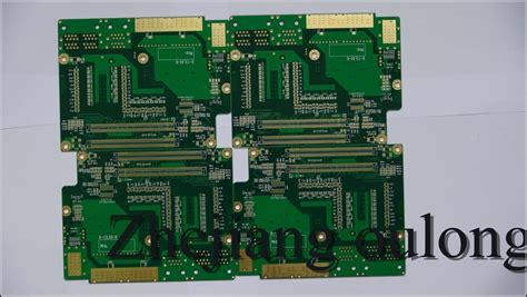
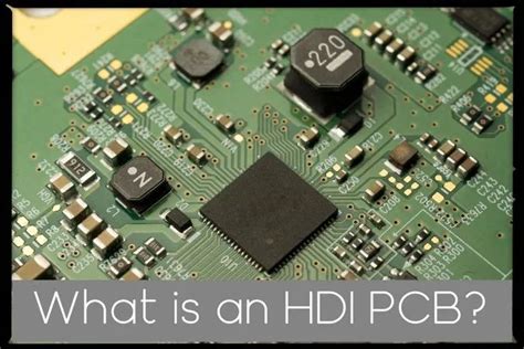
What is HDI PCB?
HDI (High Density Interconnect) PCB is a type of printed circuit board that features a higher wiring density per unit area than conventional PCBs. This is achieved through the use of smaller vias, finer traces, and advanced manufacturing techniques. HDI PCBs allow for the miniaturization of electronic devices while maintaining or improving their functionality and performance.
Key Features of HDI PCBs
- Smaller vias (microvias) with diameters less than 150μm
- Finer trace widths and spaces, typically less than 100μm
- Higher layer counts (8 or more)
- Buried and blind vias for increased Routing Density
- Sequential lamination process for building up layers
Benefits of Using HDI PCBs
Space Savings
One of the primary benefits of HDI PCBs is the significant reduction in space requirements. With the ability to route traces more densely and use smaller components, designers can create more compact devices without sacrificing functionality. This is particularly important in applications where size is a critical factor, such as mobile devices, wearables, and aerospace systems.
Improved Performance
HDI PCBs offer improved electrical performance compared to traditional PCBs. The shorter signal paths and reduced layer count result in lower signal loss, reduced crosstalk, and improved signal integrity. Additionally, the use of buried and blind vias minimizes the impact of vias on signal quality, as they do not extend through the entire thickness of the board.
Enhanced Reliability
The advanced manufacturing techniques used in HDI PCBs contribute to their enhanced reliability. The smaller vias and finer traces are less susceptible to thermal and mechanical stress, reducing the risk of failures caused by thermal cycling or vibration. Furthermore, the use of high-quality materials and strict manufacturing controls ensures that HDI PCBs can withstand harsh environmental conditions.
Cost Efficiency
Although HDI PCBs may have a higher initial cost compared to traditional PCBs, they offer long-term cost efficiency. The space savings and improved performance enable designers to create more advanced and reliable products, reducing the need for costly redesigns or repairs. Additionally, the increased routing density allows for the consolidation of multiple conventional PCBs into a single HDI PCB, reducing overall system costs.
HDI PCB Design Considerations
Material Selection
Choosing the right materials is crucial for the success of an HDI PCB design. The substrate material should have a low dielectric constant and low loss tangent to minimize signal loss and maintain signal integrity. Common materials used in HDI PCBs include FR-4, polyimide, and PTFE (Teflon). The copper foil should be of high quality and have a suitable thickness to ensure reliable trace formation and via plating.
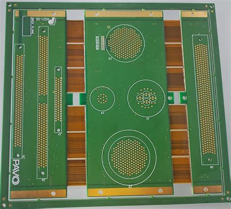
Via Types and Placement
HDI PCBs utilize various types of vias, including through-hole, blind, and buried vias. Through-hole vias extend through the entire thickness of the board, while blind vias connect an outer layer to an inner layer, and buried vias connect two or more inner layers without reaching the outer layers. The placement of vias should be carefully considered to optimize routing density and signal integrity.
Trace Width and Spacing
To achieve the high wiring density of HDI PCBs, designers must use finer trace widths and spaces. The minimum trace width and spacing depend on the manufacturing capabilities of the PCB fabricator and the electrical requirements of the design. Designers should work closely with their fabricator to determine the optimal trace dimensions for their specific application.
Layer Stack-up
The layer stack-up of an HDI PCB plays a critical role in its performance and manufacturability. Designers should carefully choose the number and arrangement of layers based on the routing requirements and signal integrity considerations. A symmetrical stack-up with equal numbers of layers on either side of the center can help minimize warpage and ensure better manufacturability.
Signal Integrity Analysis
To ensure the optimal performance of an HDI PCB, designers must conduct thorough signal integrity analysis. This involves simulating the behavior of signals as they propagate through the board and identifying potential issues such as crosstalk, reflections, and power distribution noise. Tools such as SPICE simulators and electromagnetic field solvers can assist in this process.

HDI PCB Manufacturing Process
Sequential Lamination
HDI PCBs are typically manufactured using a sequential lamination process, which involves building up the layers one at a time. This process allows for the creation of buried and blind vias, as well as the use of different materials for different layers. The sequential lamination process consists of the following steps:
- Core lamination: The initial core layers are laminated together.
- Drilling: Through-holes and blind vias are drilled in the core layers.
- Plating: The drilled holes are plated with copper to create conductive paths.
- Patterning: The outer layers are patterned using photolithography and etching techniques.
- Additional lamination: Additional layers are added by repeating steps 1-4 as needed.
Laser Drilling
Laser drilling is a key technology used in the manufacturing of HDI PCBs. Unlike mechanical drilling, laser drilling allows for the creation of much smaller vias (microvias) with diameters down to 50μm. Laser drilling is typically performed using UV or CO2 lasers, which vaporize the dielectric material to create the via holes.
Plasma Desmear
After laser drilling, the via holes must be cleaned and prepared for plating. This is accomplished through a process called plasma desmear, which uses a plasma to remove any debris or resin smear from the via walls. Plasma desmear ensures a clean and uniform surface for reliable copper plating.
Via Filling
To create a smooth surface for subsequent layer lamination, the microvias must be filled with a conductive material. This is typically done using electroplating or conductive paste filling. Electroplating involves depositing copper into the vias until they are completely filled, while conductive paste filling uses a screen printing process to fill the vias with a conductive epoxy.
Testing and Quality Control
Electrical Testing
Electrical testing is essential to ensure the functionality and reliability of an HDI PCB. Various tests are performed, including:
- Continuity test: Verifies that all connections are intact and there are no open circuits.
- Isolation test: Checks for any short circuits between adjacent traces or layers.
- Impedance test: Measures the impedance of controlled impedance traces to ensure they meet the design requirements.
- High-potential (HiPot) test: Applies a high voltage to the board to detect any insulation breakdowns or leakage currents.
Visual Inspection
Visual inspection is performed throughout the manufacturing process to identify any visible defects or anomalies. This can be done manually by trained operators or using automated optical inspection (AOI) systems. AOI systems use cameras and image processing algorithms to detect issues such as missing components, incorrect component placement, or solder bridging.
X-ray Inspection
X-ray inspection is used to detect internal defects that cannot be seen by visual inspection. This is particularly important for HDI PCBs, which have a high density of buried and blind vias. X-ray systems can identify issues such as voids in via filling, improper via registration, or delamination between layers.
Microsectioning
Microsectioning is a destructive testing method that involves cross-sectioning a sample of the PCB and examining it under a microscope. This allows for the detailed inspection of the internal structure of the board, including the quality of via plating, the integrity of the lamination, and the presence of any internal cracks or voids. Microsectioning is typically performed on a small batch of boards to ensure the manufacturing process is consistent and meets the required quality standards.
Frequently Asked Questions (FAQ)
-
What is the minimum via size achievable with HDI PCBs?
With current laser drilling technology, HDI PCBs can achieve via diameters as small as 50μm. However, the actual minimum via size depends on the specific manufacturing capabilities of the PCB fabricator and the design requirements of the project. -
Can HDI PCBs be used for high-power applications?
Yes, HDI PCBs can be used for high-power applications, but special considerations must be taken during the design and manufacturing process. This includes using thicker copper layers, providing adequate thermal management, and ensuring proper power distribution. The use of advanced materials with high thermal conductivity, such as metal-core substrates, can also help dissipate heat in high-power HDI PCBs. -
Are HDI PCBs more expensive than traditional PCBs?
In general, HDI PCBs have a higher initial cost compared to traditional PCBs due to the advanced manufacturing techniques and materials used. However, HDI PCBs offer long-term cost savings by enabling the miniaturization of devices, improving performance and reliability, and reducing the need for multiple conventional PCBs in a system. -
What are the challenges in designing HDI PCBs?
Some of the main challenges in designing HDI PCBs include: - Ensuring signal integrity in high-density layouts
- Managing thermal issues due to the compact nature of HDI PCBs
- Selecting the appropriate materials and stack-up for the specific application
- Optimizing via placement and routing for manufacturability and reliability
-
Collaborating closely with the PCB fabricator to ensure design feasibility and manufacturability
-
How long does it take to manufacture an HDI PCB?
The manufacturing time for an HDI PCB depends on various factors, such as the complexity of the design, the number of layers, and the workload of the PCB fabricator. In general, HDI PCBs take longer to manufacture than traditional PCBs due to the additional processing steps involved, such as sequential lamination and laser drilling. Typical lead times for HDI PCBs range from 2-4 weeks, but this can vary based on the specific project requirements and the fabricator’s capabilities.
Conclusion
HDI PCBs offer numerous benefits, including space savings, improved performance, enhanced reliability, and long-term cost efficiency. By understanding the key design considerations, manufacturing processes, and testing methods involved in HDI PCBs, designers can create advanced and reliable electronic devices that meet the ever-increasing demands of modern applications.
As technology continues to evolve, the importance of HDI PCBs will only grow. By staying up-to-date with the latest advancements in materials, manufacturing techniques, and design tools, electronics engineers and PCB designers can unlock the full potential of HDI PCBs and push the boundaries of what is possible in electronic packaging.
No responses yet