What is HDI PCB?
HDI PCB stands for High Density Interconnect Printed Circuit Board. It is a type of PCB that features a higher wiring density per unit area compared to conventional PCBs. HDI PCBs have finer lines and spaces, smaller vias, and capture pads, and use higher connection pad density than traditional PCBs.
The main characteristics of HDI PCBs are:
– Any density of 120 pins per square inch or more on one or both sides
– Via hole diameters of 0.006 in or less
– Capture pads of 0.012 in or less
– Line width/space of 4/4 mils or less
HDI technology enables the manufacturing of lighter, thinner, and smaller electronic products with better electrical performance. It provides a solution for applications that require high speed, high frequency, and high pin count components in a limited space.
Benefits of HDI PCB
HDI PCBs offer several advantages over traditional PCBs:
-
Reduced Size and Weight: HDI PCBs allow for miniaturization of electronic devices by incorporating more functionality into a smaller footprint. This results in lighter and more compact products.
-
Improved Electrical Performance: The shorter signal paths and reduced layer count in HDI PCBs lead to better signal integrity, lower crosstalk, and reduced electromagnetic interference (EMI).
-
Increased Reliability: HDI PCBs have smaller vias and capture pads, which reduces the risk of defects and improves the overall reliability of the circuit board.
-
Cost-Effective: Although the initial cost of HDI PCBs may be higher than traditional PCBs, they offer cost savings in the long run due to reduced assembly time, fewer components, and improved yield.
-
Faster Time-to-Market: HDI technology enables faster design and manufacturing cycles, allowing companies to bring their products to market more quickly.

HDI PCB Manufacturing Process
The manufacturing process of HDI PCBs involves several steps:
1. Design and Layout
The first step in HDI PCB manufacturing is designing the circuit board using CAD software. The design must adhere to HDI design guidelines, such as minimum via size, line width/spacing, and capture pad size.
2. Material Selection
The choice of material for HDI PCBs depends on the application requirements, such as thermal stability, dielectric constant, and loss tangent. The most common materials used are FR-4, Rogers, and Polyimide.
3. Drilling
After the design is finalized, the next step is drilling holes in the PCB substrate. HDI PCBs require smaller drill sizes compared to traditional PCBs, typically 0.006 in or less.
4. Plating
The drilled holes are then plated with copper to create vias that connect the different layers of the PCB. The plating process for HDI PCBs is more challenging due to the smaller via sizes.
5. Patterning
The copper layers are patterned using photolithography and etching processes to create the desired circuit pattern. HDI PCBs require finer feature sizes and tighter tolerances compared to traditional PCBs.
6. Lamination
The patterned layers are then laminated together using heat and pressure to form a multi-layer PCB. The lamination process for HDI PCBs requires careful control of temperature and pressure to ensure proper bonding.
7. Surface Finish
The final step is applying a surface finish to the PCB to protect the copper traces and pads from oxidation and corrosion. The most common surface finishes for HDI PCBs are ENIG (Electroless Nickel Immersion Gold) and ENEPIG (Electroless Nickel Electroless Palladium Immersion Gold).

HDI PCB Design Considerations
Designing HDI PCBs requires careful consideration of several factors to ensure optimal performance and manufacturability:
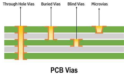
1. Via Types and Sizes
HDI PCBs use different types of vias, such as blind vias, buried vias, and micro vias, depending on the layer stack-up and routing requirements. The via sizes should be as small as possible to maximize routing density while maintaining manufacturability.
| Via Type | Definition | Typical Size Range |
|---|---|---|
| Through Hole | Drilled through the entire board thickness | 0.2 mm – 0.4 mm |
| Blind | Connects an outer layer to an inner layer | 0.1 mm – 0.15 mm |
| Buried | Connects inner layers without penetrating the surface | 0.1 mm – 0.15 mm |
| Micro | Laser-drilled, used for high-density designs | 0.05 mm – 0.1 mm |
2. Layer Stack-up
The layer stack-up of an HDI PCB depends on the number of layers, via types, and material properties. A typical HDI layer stack-up consists of a core layer, buildup layers, and microvias connecting the layers. The stack-up should be designed to minimize signal integrity issues and manufacturing complexities.
3. Trace Width and Spacing
HDI PCBs require finer trace widths and spacing compared to traditional PCBs to achieve higher routing density. The minimum trace width and spacing depend on the PCB manufacturer’s capabilities and the design requirements. A typical HDI design may have trace widths and spacing of 3-4 mils (0.075-0.1 mm).
4. Pad Size and Pitch
The pad size and pitch of components on HDI PCBs should be minimized to increase routing density. However, the pad size should be large enough to ensure reliable soldering and assembly. The pitch, which is the distance between the centers of adjacent pads, should be as small as possible while maintaining manufacturability.
5. Signal Integrity
HDI PCBs are often used in high-speed applications where signal integrity is critical. Designers must consider factors such as impedance matching, crosstalk, and EMI when designing HDI PCBs. Techniques such as differential routing, ground planes, and shielding can be used to improve signal integrity.

HDI PCB Testing and Inspection
Testing and inspection are crucial steps in ensuring the quality and reliability of HDI PCBs. Some common testing and inspection methods include:
1. Automated Optical Inspection (AOI)
AOI uses cameras and image processing algorithms to inspect the PCB for defects such as missing components, solder bridges, and incorrect component placement.
2. X-ray Inspection
X-ray inspection is used to detect internal defects such as voids in vias, delamination, and cracks that are not visible from the surface.
3. Electrical Testing
Electrical testing is performed to verify the functionality and performance of the PCB. This includes continuity testing, insulation resistance testing, and high-potential testing.
4. Microsectioning
Microsectioning involves cross-sectioning the PCB and examining the internal structure using microscopy techniques. This method is used to assess the quality of vias, plating, and lamination.
Applications of HDI PCB
HDI PCBs are widely used in various industries and applications that require high-density, high-performance electronic packaging. Some common applications include:
- Consumer Electronics: Smartphones, tablets, wearables, and other portable devices.
- Automotive Electronics: Advanced driver assistance systems (ADAS), infotainment systems, and vehicle control units.
- Medical Devices: Implantable devices, diagnostic equipment, and wearable health monitors.
- Aerospace and Defense: Avionics, radar systems, and satellite communications.
- Industrial Automation: Robotics, machine vision systems, and process control equipment.
FAQ
1. What is the difference between HDI PCB and traditional PCB?
HDI PCBs have higher wiring density, finer lines and spaces, smaller vias and capture pads compared to traditional PCBs. This allows for the miniaturization of electronic devices and improved electrical performance.
2. What are the advantages of using HDI PCB?
The advantages of using HDI PCBs include reduced size and weight, improved electrical performance, increased reliability, cost-effectiveness, and faster time-to-market.
3. What materials are commonly used for HDI PCB substrates?
The most common materials used for HDI PCB substrates are FR-4, Rogers, and Polyimide. The choice of material depends on the application requirements, such as thermal stability, dielectric constant, and loss tangent.
4. What are the different types of vias used in HDI PCBs?
HDI PCBs use different types of vias, such as blind vias, buried vias, and micro vias, depending on the layer stack-up and routing requirements. Blind vias connect an outer layer to an inner layer, buried vias connect inner layers without penetrating the surface, and micro vias are laser-drilled for high-density designs.
5. What are the testing and inspection methods used for HDI PCBs?
Common testing and inspection methods for HDI PCBs include automated optical inspection (AOI), X-ray inspection, electrical testing, and microsectioning. These methods are used to detect defects, verify functionality, and assess the quality of the PCB.
Conclusion
HDI PCB technology has revolutionized the electronics industry by enabling the manufacturing of smaller, lighter, and higher-performance devices. The increased wiring density, finer features, and advanced via structures of HDI PCBs offer numerous benefits, such as improved electrical performance, increased reliability, and faster time-to-market.
However, designing and manufacturing HDI PCBs requires careful consideration of various factors, such as via types and sizes, layer stack-up, trace width and spacing, pad size and pitch, and signal integrity. Proper testing and inspection methods are also crucial to ensure the quality and reliability of HDI PCBs.
As electronic devices continue to become more complex and compact, the demand for HDI PCBs will only continue to grow. By understanding the principles, benefits, and challenges of HDI PCB technology, designers and manufacturers can create innovative and high-performance electronic products that meet the evolving needs of various industries and applications.
No responses yet