Introduction to Gerber Files
Gerber files are the standard file format used in the printed circuit board (PCB) industry for the design and manufacture of PCBs. They contain all the necessary information for the fabrication of a PCB, including the copper layers, solder mask, silkscreen, and drill data. Gerber files are essential for communicating the design intent to the PCB manufacturer and ensuring that the final product meets the desired specifications.
In this comprehensive guide, we will walk you through the process of generating Gerber files step by step. We will cover the basics of Gerber file format, the tools and software required, and the best practices for creating high-quality Gerber files. By the end of this article, you will have a solid understanding of how to generate Gerber files and be well-equipped to tackle your next PCB design project.
What are Gerber Files?
Gerber files are named after the Gerber Scientific Instrument Company, which developed the Gerber format in the 1960s. The Gerber format has since become the de facto standard for the PCB industry. Gerber files are ASCII text files that contain vector information for each layer of a PCB. They use a series of commands to define the shapes, lines, and pads on each layer.
Gerber files typically consist of several individual files, each representing a specific layer or aspect of the PCB design. These files include:
- Copper layers (e.g., TOP.gbr, BOTTOM.gbr)
- Solder mask layers (e.g., SMTOP.gbr, SMBOT.gbr)
- Silkscreen layers (e.g., SSTOP.gbr, SSBOT.gbr)
- Drill data (e.g., DRILL.drl)
- Board outline (e.g., OUTLINE.gbr)
Each Gerber file contains a series of commands that define the features on that specific layer. These commands include aperture definitions (e.g., D10), tool selections (e.g., D10), and coordinate data (e.g., X1000Y1500D02).

Tools and Software for Generating Gerber Files
To generate Gerber files, you will need a PCB design software package that supports Gerber file export. Some popular PCB design software options include:
- Altium Designer
- Eagle
- KiCad
- OrCAD
- PADS
Most of these software packages have built-in Gerber File Generation capabilities, allowing you to easily export your PCB design as a set of Gerber files.
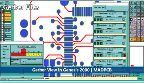
In addition to PCB design software, there are also standalone Gerber file viewers and editors that can be used to inspect and modify Gerber files. Some popular options include:
- GC-Prevue
- ViewMate
- GerbView (included with KiCad)
- CamView
These tools can be useful for verifying the correctness of your Gerber files before sending them to the PCB manufacturer.

Step-by-Step Guide to Generating Gerber Files
Now that we have covered the basics of Gerber files and the tools required, let’s dive into the step-by-step process of generating Gerber files.
Step 1: Complete Your PCB Design
Before generating Gerber files, you must first complete your PCB design in your chosen PCB design software. This includes placing components, routing traces, defining pad sizes and shapes, and adding any necessary text or graphics.
Step 2: Set Up Your Gerber File Export Settings
Once your PCB design is complete, you need to set up your Gerber file export settings. This typically involves specifying the following:
- Output directory: Where the Gerber files will be saved
- File format: RS-274X is the most common Gerber file format
- Units: Inches or millimeters
- Aperture list: Include aperture list in the Gerber files
- Decimal places: Number of decimal places for coordinates (usually 4 or 5)
Each PCB design software package will have its own specific steps for setting up Gerber file export settings. Consult your software’s documentation for detailed instructions.
Step 3: Export Individual Gerber Files
With your Gerber file export settings configured, you can now export the individual Gerber files for each layer of your PCB design. This typically involves selecting the layers you want to export and clicking an “Export” or “Generate” button.
Here’s an example of how to export Gerber files in Altium Designer:
- Go to File > Fabrication Outputs > Gerber Files
- In the Gerber Setup dialog, specify the output directory and file format
- Select the layers you want to export (e.g., Top Layer, Bottom Layer, Top Solder Mask, etc.)
- Click “OK” to generate the Gerber files
Repeat this process for each layer of your PCB design until you have a complete set of Gerber files.
Step 4: Verify Your Gerber Files
After generating your Gerber files, it’s crucial to verify that they are correct and free of errors. This can be done using a Gerber file viewer or editor.
Here are some key things to check when verifying your Gerber files:
- Aperture list: Ensure that all apertures are defined and used correctly
- Drill data: Check that all drill holes are present and sized correctly
- Board outline: Verify that the board outline is correct and matches your design
- Alignment: Check that all layers align correctly with each other
If you find any errors or discrepancies, make the necessary corrections in your PCB design software and re-export the Gerber files.
Step 5: Package and Send Your Gerber Files
Once you have verified your Gerber files, the final step is to package them and send them to your PCB manufacturer. Most manufacturers will require you to zip or compress your Gerber files into a single archive file.
When sending your Gerber files to the manufacturer, be sure to include any additional information or specifications they may require, such as:
- PCB thickness
- Copper weight
- Solder mask color
- Silkscreen color
- Surface finish (e.g., HASL, ENIG, etc.)

Best Practices for Generating Gerber Files
To ensure the best possible results when generating Gerber files, follow these best practices:
- Use a consistent naming convention for your Gerber files (e.g., PCB_Top_Layer.gbr, PCB_Bottom_Layer.gbr, etc.)
- Include an aperture list in your Gerber files to ensure that all apertures are defined correctly
- Use a high-resolution export settings (e.g., 4 or 5 decimal places) to avoid rounding errors
- Always verify your Gerber files before sending them to the manufacturer
- Communicate clearly with your PCB manufacturer and provide all necessary information and specifications
By following these best practices, you can minimize the risk of errors and ensure a smooth PCB fabrication process.
Common Gerber File Generation Mistakes and How to Avoid Them
Despite best efforts, mistakes can happen when generating Gerber files. Here are some common mistakes and how to avoid them:
-
Incorrect layer selection: Make sure to select all necessary layers when exporting Gerber files, including copper layers, solder mask, silkscreen, and drill data.
-
Incorrect units: Ensure that your Gerber files use the correct units (inches or millimeters) and that they match the units used in your PCB design software.
-
Missing or incorrect aperture definitions: Double-check that all apertures are defined correctly in your Gerber files and that they match the apertures used in your PCB design.
-
Incorrect board outline: Verify that the board outline in your Gerber files matches the board outline in your PCB design.
-
Incomplete or missing drill data: Make sure to include all necessary drill data in your Gerber files, including the drill sizes and locations.
To avoid these mistakes, always double-check your Gerber files before sending them to the manufacturer, and use a Gerber file viewer or editor to verify their correctness.
Frequently Asked Questions (FAQ)
- What is the difference between Gerber files and ODB++ files?
-
Gerber files are the standard file format for PCB fabrication, while ODB++ is a newer, more comprehensive format that includes additional information such as component placement and netlist data. While some PCB manufacturers may accept ODB++ files, Gerber files are still the most widely used and accepted format.
-
Can I use different PCB design software to generate Gerber files?
-
Yes, most PCB design software packages support Gerber file export, including Altium Designer, Eagle, KiCad, OrCAD, and PADS. The specific steps for generating Gerber files may vary slightly between software packages, but the overall process is similar.
-
What should I do if my PCB manufacturer reports an issue with my Gerber files?
-
If your PCB manufacturer reports an issue with your Gerber files, the first step is to communicate with them to understand the specific problem. They may provide feedback or instructions on how to correct the issue. If necessary, make the required changes in your PCB design software and re-export the Gerber files.
-
How do I ensure that my Gerber files are compatible with my PCB manufacturer’s requirements?
-
To ensure compatibility with your PCB manufacturer’s requirements, it’s best to communicate with them directly and obtain their specific Gerber file requirements, such as file format, units, and aperture list format. Many manufacturers also provide Gerber file templates or guidelines that you can follow.
-
What is the best resolution to use when exporting Gerber files?
- The recommended resolution for exporting Gerber files is 4 or 5 decimal places. This ensures a high level of precision and minimizes the risk of rounding errors. However, it’s always a good idea to consult with your PCB manufacturer to confirm their preferred resolution settings.
Conclusion
Generating Gerber files is a critical step in the PCB design and fabrication process. By understanding the Gerber file format, using the right tools and software, and following best practices, you can ensure that your Gerber files are accurate, complete, and ready for manufacturing.
Remember to always verify your Gerber files before sending them to the manufacturer, and communicate clearly to avoid any potential issues or delays. With practice and attention to detail, generating high-quality Gerber files will become a smooth and efficient process, helping you bring your PCB designs to life.
No responses yet