Introduction to EMI Prevention
Electromagnetic interference (EMI) is a common problem in electronic devices that can cause malfunctions, signal degradation, and even complete system failure. EMI occurs when unwanted electromagnetic energy interferes with the normal operation of an electronic device. This interference can come from a variety of sources, including power lines, radio transmitters, and other electronic devices.
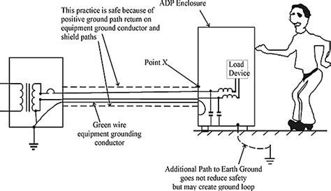
To prevent EMI, designers must carefully consider the layout and design of their circuits, particularly the ground return path. The ground return path is the path that current takes to return to its source, and it plays a critical role in minimizing EMI. In this article, we will explore the importance of following your multilayer ground return path to prevent EMI and discuss strategies for designing effective ground return paths.
Understanding the Ground Return Path
The ground return path is the path that current takes to return to its source. In a typical electronic circuit, current flows from the power supply, through the load, and back to the power supply through the ground return path. The ground return path is usually a low-impedance path that is designed to minimize resistance and inductance.
The importance of the ground return path cannot be overstated. A poorly designed ground return path can lead to a variety of problems, including:
- Ground bounce: Ground bounce occurs when the voltage on the ground plane fluctuates due to rapid changes in current flow. This can cause false triggering of logic gates and other components.
- EMI: A poorly designed ground return path can act as an antenna, radiating electromagnetic energy and causing EMI.
- Signal integrity issues: A poorly designed ground return path can cause signal integrity issues, such as crosstalk and reflections.
To minimize these problems, designers must carefully consider the layout and design of the ground return path.

Designing Effective Ground Return Paths
Designing effective ground return paths requires careful consideration of several factors, including:
- Impedance: The impedance of the ground return path should be as low as possible to minimize resistance and inductance.
- Current density: The current density of the ground return path should be carefully considered to avoid hot spots and minimize EMI.
- Routing: The routing of the ground return path should be carefully considered to minimize loop areas and avoid coupling with other signals.
One effective strategy for designing ground return paths is to use a multilayer PCB. A multilayer PCB allows designers to create separate ground planes for different sections of the circuit, minimizing coupling and reducing EMI. By carefully routing signals and power traces on different layers, designers can create a low-impedance ground return path that minimizes EMI and ensures signal integrity.
Another important consideration when designing ground return paths is the use of ground vias. Ground vias are used to connect ground planes on different layers of the PCB, creating a low-impedance path for current to flow. By strategically placing ground vias near high-speed signals and power traces, designers can minimize loop areas and reduce EMI.
| Layer | Purpose |
|---|---|
| Top | Signal traces, components |
| Ground | Ground plane |
| Power | Power plane |
| Bottom | Signal traces, components |
Table 1: Example of a four-layer PCB stackup

Common EMI Sources and Mitigation Strategies
There are several common sources of EMI that designers must be aware of when designing electronic devices. These include:
- Power supplies: Power supplies can generate significant amounts of EMI, particularly if they are not properly filtered and decoupled.
- High-speed signals: High-speed signals, such as clock signals and data buses, can generate significant amounts of EMI if they are not properly terminated and routed.
- Electrostatic discharge (ESD): ESD events can generate significant amounts of EMI and can damage sensitive electronic components.
To mitigate these sources of EMI, designers can use a variety of strategies, including:
- Filtering and decoupling: Power supplies should be properly filtered and decoupled to minimize EMI. This can be achieved using capacitors, inductors, and other passive components.
- Termination and routing: High-speed signals should be properly terminated and routed to minimize reflections and crosstalk. This can be achieved using techniques such as impedance matching and differential signaling.
- Shielding: Sensitive components and circuits can be shielded using metal enclosures or conductive coatings to minimize EMI.
| EMI Source | Mitigation Strategy |
|---|---|
| Power supplies | Filtering and decoupling |
| High-speed signals | Termination and routing |
| ESD | Shielding, ESD protection devices |
Table 2: Common EMI sources and mitigation strategies

Case Study: Designing a High-Speed Digital Interface
To illustrate the importance of following your multilayer ground return path to prevent EMI, let’s consider a case study of designing a high-speed digital interface.
Suppose we are designing a device that includes a high-speed digital interface, such as a USB 3.0 port. USB 3.0 operates at speeds up to 5 Gbps, which can generate significant amounts of EMI if not properly designed.
To minimize EMI, we will use a four-layer PCB with separate ground planes for the digital and analog sections of the circuit. We will route the USB 3.0 signals on the top layer of the PCB, with a ground plane directly beneath them to minimize loop areas and provide a low-impedance return path.
We will also use differential signaling for the USB 3.0 data lines to minimize crosstalk and EMI. Differential signaling uses two signal lines that are 180 degrees out of phase with each other, canceling out any EMI that is generated.
To further minimize EMI, we will use ground vias to connect the ground planes on different layers of the PCB. We will place ground vias near the USB 3.0 connector to provide a low-impedance path for current to flow back to the source.
By carefully designing the ground return path and using techniques such as differential signaling and ground vias, we can minimize EMI and ensure reliable operation of the USB 3.0 interface.
Frequently Asked Questions (FAQ)
- What is EMI and why is it important to prevent it?
-
EMI stands for electromagnetic interference, which is the unwanted disturbance caused by electromagnetic radiation emitted by electronic devices. It is important to prevent EMI because it can cause malfunctions, signal degradation, and even complete system failure in electronic devices.
-
What is the ground return path and why is it important?
-
The ground return path is the path that current takes to return to its source in an electronic circuit. It is important because a poorly designed ground return path can lead to problems such as ground bounce, EMI, and signal integrity issues.
-
How can a multilayer PCB help prevent EMI?
-
A multilayer PCB can help prevent EMI by allowing designers to create separate ground planes for different sections of the circuit, minimizing coupling and reducing EMI. By carefully routing signals and power traces on different layers, designers can create a low-impedance ground return path that minimizes EMI and ensures signal integrity.
-
What are some common sources of EMI and how can they be mitigated?
-
Common sources of EMI include power supplies, high-speed signals, and electrostatic discharge (ESD) events. These sources can be mitigated using techniques such as filtering and decoupling for power supplies, termination and routing for high-speed signals, and shielding and ESD protection devices for ESD events.
-
What are some techniques for designing effective ground return paths?
- Some techniques for designing effective ground return paths include using a multilayer PCB with separate ground planes, carefully considering impedance and current density, strategically placing ground vias, and using differential signaling for high-speed signals. By carefully designing the ground return path, designers can minimize EMI and ensure reliable operation of electronic devices.
Conclusion
Preventing EMI is critical for ensuring the reliable operation of electronic devices. One of the most effective strategies for minimizing EMI is to carefully design the ground return path. By using a multilayer PCB with separate ground planes, strategically placing ground vias, and using differential signaling for high-speed signals, designers can create a low-impedance ground return path that minimizes EMI and ensures signal integrity.
When designing electronic devices, it is important to consider the various sources of EMI and use appropriate mitigation strategies, such as filtering and decoupling for power supplies, termination and routing for high-speed signals, and shielding and ESD protection devices for ESD events.
By following these strategies and carefully designing the ground return path, designers can create electronic devices that are reliable, efficient, and free from EMI. As electronic devices continue to become more complex and high-speed, the importance of effective EMI prevention strategies will only continue to grow.
No responses yet