Introduction to High-tech PCB
In today’s rapidly advancing technological landscape, the demand for high-performance electronic devices has never been greater. At the heart of these devices lie the printed circuit boards (PCBs) that enable their functionality. As the electronics industry continues to push the boundaries of what is possible, the focus has shifted towards high layer, high frequency, high-speed PCB, advanced PCBA, and original components. These cutting-edge technologies are revolutionizing the way we design and manufacture electronic devices, enabling faster, more efficient, and more reliable performance.
What is a High Layer PCB?
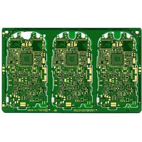
A high layer PCB is a printed circuit board that consists of multiple layers of conductive material, typically copper, separated by insulating layers. The number of layers in a high layer PCB can range from 8 to 40 or more, depending on the complexity of the design and the requirements of the application. The increased number of layers allows for more complex routing of signals and power, as well as improved signal integrity and reduced electromagnetic interference (EMI).
| Number of Layers | Typical Applications |
|---|---|
| 8-12 | High-speed digital devices, telecommunications equipment |
| 14-20 | Advanced computer systems, aerospace and defense electronics |
| 22-30 | High-density interconnect (HDI) devices, medical equipment |
| 32-40+ | Cutting-edge research and development, specialized applications |
Advantages of High Layer PCBs
- Increased routing density: With more layers available, designers can route signals and power more efficiently, allowing for more complex designs in a smaller footprint.
- Improved signal integrity: The increased number of layers allows for better control over signal paths, reducing crosstalk and improving signal quality.
- Enhanced thermal management: Multiple layers can be dedicated to power and ground planes, providing better heat dissipation and reducing thermal stress on components.
- Reduced EMI: The increased number of layers allows for better shielding and grounding, reducing electromagnetic interference and improving overall system performance.
High Frequency PCB Design Considerations
High frequency PCBs are designed to operate at frequencies above 1 GHz, which presents unique challenges in terms of signal integrity, power management, and EMI control. When designing high frequency PCBs, several key factors must be considered to ensure optimal performance.
Material Selection
The choice of substrate material is crucial in high frequency PCB design. The material must have a low dielectric constant (Dk) and low dissipation factor (Df) to minimize signal loss and distortion. Some common high frequency substrate materials include:
- Rogers RO4000 series: A hydrocarbon ceramic laminate with excellent high frequency performance and low cost.
- Isola IS680: A low-loss, high-speed laminate with good thermal stability and CAF resistance.
- PTFE (Teflon): A low-loss material with excellent high frequency performance, but higher cost and more difficult to process.
Controlled Impedance
Maintaining consistent impedance throughout the signal path is essential for high frequency PCBs. Impedance mismatches can cause signal reflections, leading to signal distortion and degraded performance. Controlled impedance is achieved through careful design of trace widths, spacing, and layer stackup.
Grounding and Shielding
Proper grounding and shielding techniques are critical in high frequency PCB design to minimize EMI and ensure signal integrity. Some best practices include:
- Use of ground planes to provide a low-impedance return path for high frequency signals.
- Placement of decoupling capacitors close to power pins to reduce high frequency noise.
- Use of shielding techniques, such as via fencing and ground stitching, to contain high frequency signals and prevent unwanted radiation.

High-speed PCB Design Techniques
High-speed PCBs are designed to transmit signals at high data rates, typically above 1 Gbps. At these speeds, signal integrity becomes a primary concern, as even small discontinuities in the signal path can cause significant signal degradation. To ensure optimal performance, several design techniques must be employed.
Differential Signaling
Differential signaling is a technique where two complementary signals are transmitted on separate traces, with the signal being the difference between the two. This approach offers several advantages over single-ended signaling:
- Improved noise immunity: Common-mode noise is canceled out, as it affects both signals equally.
- Reduced EMI: The complementary signals create opposing electromagnetic fields, minimizing radiation.
- Higher data rates: Differential signals can be transmitted at higher speeds without suffering from significant signal degradation.
Length Matching
In high-speed PCBs, it is crucial to ensure that signal paths are of equal length to maintain signal integrity. Length mismatches can cause signal skew, leading to timing errors and reduced performance. Length matching is achieved through careful routing and the use of serpentine traces to add controlled amounts of delay.
Via Optimization
Vias are used to connect traces between layers in a PCB, but they can also cause signal reflections and degradation at high speeds. To minimize these effects, several via optimization techniques can be employed:
- Use of microvias: Smaller vias that span fewer layers, reducing the discontinuity in the signal path.
- Back-drilling: Removing the unused portion of a via to reduce the stub length and minimize reflections.
- Via stitching: Adding additional vias around signal vias to provide a low-impedance return path and reduce EMI.

Advanced PCBA Processes
Advanced printed circuit board assembly (PCBA) processes are essential for realizing the full potential of high layer, high frequency, and high-speed PCBs. These processes ensure the precise placement and reliable attachment of components, as well as the protection of the assembled board from environmental stresses.
Surface Mount Technology (SMT)
SMT is the dominant assembly process for modern PCBs, offering several advantages over through-hole technology:
- Higher component density: SMT components are smaller and can be placed on both sides of the board, enabling more compact designs.
- Faster assembly: SMT components are placed and soldered using automated equipment, reducing assembly time and cost.
- Improved reliability: SMT components have shorter leads and are more securely attached to the board, improving reliability and resistance to vibration and shock.
Automated Optical Inspection (AOI)
AOI is a critical quality control process in advanced PCBA, using high-resolution cameras and sophisticated algorithms to detect assembly defects such as:
- Missing or misaligned components
- Solder bridges or insufficient solder
- Reversed or incorrect components
AOI systems can inspect assembled boards quickly and accurately, reducing the need for manual inspection and improving overall quality.
Conformal Coating
Conformal coating is a process where a thin, protective layer is applied to the assembled PCB to protect it from environmental stresses such as moisture, dust, and chemicals. Common conformal coating materials include:
- Acrylic: A general-purpose coating with good moisture resistance and easy application and removal.
- Silicone: A highly flexible coating with excellent high-temperature performance and good chemical resistance.
- Parylene: A thin, conformal coating applied through a vapor deposition process, offering excellent protection against moisture and corrosion.

Original Component Selection
The selection of original, high-quality components is essential for ensuring the performance, reliability, and longevity of high-tech PCBs. When choosing components, several factors must be considered:
Manufacturer Reputation
Choosing components from reputable manufacturers with a proven track record of quality and reliability is crucial. Counterfeit or substandard components can lead to premature failure and compromised performance.
Datasheets and Specifications
Careful review of component datasheets and specifications is necessary to ensure that the chosen components meet the requirements of the design in terms of electrical characteristics, thermal performance, and package compatibility.
Availability and Lead Time
Component availability and lead times must be considered to ensure that production schedules can be met. Establishing strong relationships with component suppliers and distributors can help ensure a reliable supply chain.
Cost and Value
While cost is always a consideration in component selection, it must be balanced against the value provided by the component in terms of performance, reliability, and long-term availability. Choosing the lowest-cost option may result in compromised performance or increased risk of obsolescence.
FAQs
-
Q: What are the benefits of using a high layer PCB?
A: High layer PCBs offer several benefits, including increased routing density, improved signal integrity, enhanced thermal management, and reduced EMI. -
Q: What are some common high frequency substrate materials?
A: Common high frequency substrate materials include Rogers RO4000 series, Isola IS680, and PTFE (Teflon). -
Q: Why is length matching important in high-speed PCB design?
A: Length matching is important in high-speed PCB design to ensure that signal paths are of equal length, minimizing signal skew and maintaining signal integrity. -
Q: What are the advantages of surface mount technology (SMT) in advanced PCBA?
A: SMT offers several advantages in advanced PCBA, including higher component density, faster assembly, and improved reliability. -
Q: What factors should be considered when selecting original components for high-tech PCBs?
A: When selecting original components for high-tech PCBs, factors such as manufacturer reputation, datasheets and specifications, availability and lead time, and cost and value should be considered.
Conclusion
The development of high layer, high frequency, high-speed PCBs, advanced PCBA processes, and the selection of original components are crucial for enabling the next generation of high-performance electronic devices. By understanding the key design considerations, assembly techniques, and component selection criteria, engineers and manufacturers can create PCBs that push the boundaries of what is possible in terms of speed, reliability, and functionality.
As technology continues to advance, the importance of these high-tech PCB solutions will only continue to grow. By staying at the forefront of these developments and continually refining their processes and expertise, companies can position themselves as leaders in the industry and contribute to the ongoing revolution in electronic device performance.
No responses yet