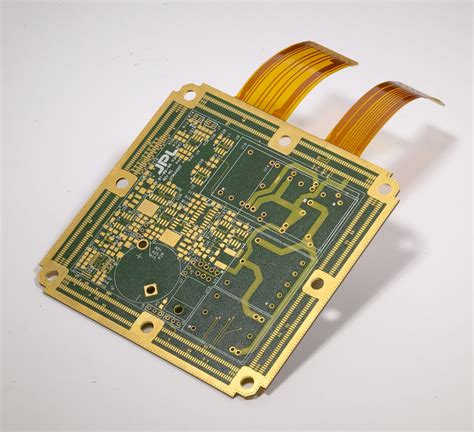
Overview of the Flex PCB Manufacturing Process
The basic steps in manufacturing a flexible printed circuit board are:
- Creating the circuit design and layout
- Printing the circuit pattern on the base material
- Etching away excess copper to define circuit traces
- Laminating protective coverlay over the circuits
- Cutting the flex PCB out into its final shape
- Surface finishing exposed metal areas
- Testing and inspecting the completed flex PCB
Each of these steps requires specialized equipment and careful process control to produce reliable, high-quality flexible circuits. Let’s examine each stage of FlexPCB-Manufacturing in more detail.
Circuit Design and Layout
Like rigid PCBs, the flex PCB manufacturing process begins with creating the circuit schematic and layout. However, designers must account for the unique properties and requirements of flexible circuits:
- Thinner copper foil and dielectric materials are used (typically 0.5-3 mils thick)
- Circuits must be designed to withstand repeated bending and flexing
- Traces and spacing are adjusted for material flexibility
- Mechanical stress on solder joints must be minimized
- Stiffeners are added in areas that should not flex
Specialist PCB design software is used to create the circuit layout and generate files to drive the manufacturing process. The output is a set of digital images or photomasks defining the copper traces, solder mask, legend, and drill data.

Printing the Circuit Pattern
With the circuit layout finalized, the first step in physically making the flex PCB is printing the circuit pattern onto the base material. There are two main methods:
- Print and etch
- Adhesiveless Lamination
Print and Etch Method
The print and etch method starts with flexible copper-clad laminate (FCCL) consisting of a thin layer of copper foil bonded to a flexible polymer substrate like polyimide. A photoresist is applied and the circuit image is printed onto it using high-resolution photomasks.
After exposure to UV light, the photoresist is developed, leaving behind a resist pattern matching the circuit traces. This etch resist will protect copper that forms the circuits in the next step.
Adhesiveless Lamination
An alternative is adhesiveless lamination, where the circuit is built up by laminating traces and pads onto the base film. The process is:
- Flexible film is coated with a seed layer (thin conductive coating)
- Photoresist is applied and patterned with the circuit image
- Additional copper is electroplated onto exposed seed layer to build up traces
- Photoresist is stripped off
- Seed layer is etched away, leaving only copper traces behind
This method avoids a separate etching step and produces finer traces than print and etch. The choice of method depends on the application and circuit requirements.

Etching Circuit Traces
For print and etch processing, the next step is to chemically etch away the unwanted copper, leaving only the resist-protected traces behind. The FCCL panel is immersed in an etching solution, typically cupric chloride or ammoniacal, which dissolves exposed copper.
Careful control of the etching process is critical to achieve traces with the right width, spacing, and integrity. Factors include:
- Etchant chemistry and concentration
- Solution temperature
- Spray pressure
- Etching time
After etching is completed, the remaining etch resist is stripped off, revealing the final copper circuit traces. The panel may go through additional processes like via hole drilling and plating at this stage.

Coverlay Lamination
To protect the delicate circuits, a thin insulating layer called coverlay is laminated on top. Coverlay is typically polyimide or polyester film with a heat-activated adhesive on one side.
The coverlay is aligned with the circuit panel and run through a heated roll laminator under controlled pressure and temperature. The adhesive flows and bonds the coverlay to the base material.
Openings in the coverlay are needed to access contact pads and other features. These are created by:
- Punching or laser cutting before lamination
- Photoimaging and developing like solder mask
- Laser cutting after lamination
The choice of method depends on the size, shape, and quantity of openings required. Tight registration between the coverlay and circuit traces is essential.
Cutting and Profiling
After lamination, the next step is cutting the panel into individual flex PCBs. There are several methods used depending on the shape and quantity:
- Steel rule die cutting
- Laser cutting
- Routing
- Punching
Steel rule die cutting is fast and economical for simple shapes and high volumes. The die is made by bending sharpened steel strips into the desired outline and mounting them in a rigid base. The panel is placed on the die and a press rams a cutting plate down, cutting through the flex material.
Laser cutting is better for intricate outlines and smaller quantities. A focused laser beam ablates the material along a programmed path to cut out the flex PCB.
Routing and punching resemble conventional PCB depaneling. Routing uses a spinning blade to cut along a path, while punching uses shaped cutting tools and a press. Care is needed to avoid stressing or deforming the flexible materials.
After cutting, the flex PCBs are separated from the processing panel. An annular ring cutter may be used to remove any remaining tab or web.
Surface Finishes
To protect exposed copper features like pads and contacts, a surface finish is applied. Common finishes for flex PCBs include:
- ENIG (Electroless Nickel Immersion Gold)
- ENEPIG (Electroless Nickel Electroless Palladium Immersion Gold)
- OSP (Organic Solderability Preservatives)
- Immersion silver
- Immersion tin
The choice of finish depends on the operating environment, contact requirements, and soldering processes to be used. ENIG and ENEPIG provide good durability and shelf life but require more processing steps. OSP, immersion silver, and tin are simpler and cheaper but have limitations.
The surface finish is applied by immersing the flex PCBs in a sequence of chemical baths under controlled conditions. Proper cleaning and process control are essential for a consistent, defect-free finish.
Testing and Inspection
The final step in FlexPCB-Manufacturing is testing and inspection to ensure the flex PCBs meet all functional and quality requirements. Some common tests include:
- Continuity and shorts testing
- Impedance testing
- Insulation resistance
- Microsectioning
- Visual inspection
- Dimensional verification
Automated test equipment and inspection systems are used to quickly check large numbers of flex PCBs. Electrical flying probe testers check for opens and shorts. Impedance testing ensures controlled impedance traces meet spec. Microsectioning evalutes plating quality and circuit integrity in cross-section.
Visual inspection, manually or by automated optical inspection (AOI), checks for surface defects like contamination, blisters, and color irregularities. Dimensional measurements using coordinate measuring machines or vision systems verify that features are within tolerances.
Flex PCBs that pass testing and inspection are ready for final packaging and shipment to the customer. Traceability markings and documentation are important for quality control.
Flex PCB Manufacturing Processes Compared
This table summarizes the key steps and methods used in manufacturing flex PCBs:
| Process Step | Methods |
|---|---|
| Circuit printing | – Print and etch – Adhesiveless lamination |
| Circuit etching | – Cupric chloride – Alkaline etchant |
| Coverlay lamination | – Adhesive lamination – Photoimaging |
| Cutting/Profiling | – Steel rule die – Laser cutting – Routing – Punching |
| Surface finish | – ENIG – ENEPIG – OSP – Immersion Ag, Sn |
| Testing | – Continuity – Shorts – Impedance – Microsection – AOI |
The choice of methods at each step depends on the specific flex PCB design, performance requirements, and production volume and cost targets.
Frequently Asked Questions
What materials are used to make flexible PCBs?
Flex PCBs are made by patterning metal circuits on thin, flexible polymer substrates. The most common base materials are polyimide (Kapton) and polyester. Polyimide is known for its high heat resistance, while polyester has good flexibility and lower cost. Copper foil is the primary conductor material, typically in thicknesses from 9 μm to 70 μm (1/3 oz to 2 oz).
What are the key advantages of flex PCBs over rigid PCBs?
Flex PCBs offer several advantages over traditional rigid PCBs:
– Lighter weight and less space through thinner materials
– Able to bend and fold to fit in tight, compact spaces
– Can flex and move with stresses, improving reliability
– Replaces wiring harnesses and connectors, simplifying assembly
– Dissipates heat better through unenclosed structure
– Enables dynamic flexing for moving parts and hinges
How small of features can be made on flex PCBs?
Flex PCBs can achieve much finer circuit features than rigid PCBs due to the thinner materials and advanced processing methods. Minimum trace widths and spaces down to 25 μm (1 mil) are possible. Adhesiveless lamination and photoimaging allow even smaller features below 10 μm. Microvias as small as 50 μm in flexible materials enable high-density interconnect.
What standards and certifications apply to flex PCBs?
Several industry standards define requirements and test methods for flex PCBs:
- IPC-6013: Qualification and Performance Specification for Flexible Printed Boards
- IPC-4203: Adhesive Coated Dielectric Films for Use as Cover Sheets for Flexible Printed Circuitry and Flexible Adhesive Bonding Films
- IPC-4202: Flexible Base Dielectrics for Use in Flexible Printed Circuitry
- IPC-4204: Flexible Metal-Clad Dielectrics for Use in Fabrication of Flexible Printed Circuitry
- ASTM F1683: Standard Practice for Bending Flexible Printed Circuit Boards for Installation Purposes
Flex PCB manufacturers can be certified to these standards by passing audits of their processes and quality systems. Certifications demonstrate a supplier’s capabilities and reduce risk for customers.
What are some common applications for flex PCBs?
Flex PCBs are used in a wide range of products and industries wherever tight packaging, light weight, or flexing are needed. Some leading applications include:
- Mobile phones and wearable electronics
- Digital cameras
- Laptops and tablets
- Medical implants and diagnostic tools
- Automotive electronics and sensors
- Aerospace and defense systems
- Industrial automation and robotics
- Internet of things (IoT) devices
As electronic products get smaller and more capabilities are squeezed into compact form factors, the use of flex PCBs will only grow. Advances in materials and FlexPCB-Manufacturing processes are enabling innovative new applications every day.
Conclusion
Flexible printed circuit boards are a remarkable technology that literally bends the rules of conventional electronics. By patterning circuits on pliable polymer films, flex PCBs can fit in tight spaces, survive the stresses of moving parts, and take on three-dimensional shapes.
Making a flex PCB is a multi-step process that converts the designer’s concept into a reliable, manufacturable product. Careful selection of materials, printing and etching processes, and inspection criteria are needed to ensure the flex PCBs will perform flawlessly.
As demand grows for wearable electronics, IoT devices, and ever smaller gadgets, flex PCBs will be at the heart of these products. With ongoing advances in FlexPCB-Manufacturing, these versatile circuits will help push the boundaries of what is possible in electronic packaging.
No responses yet