Introduction to Flex PCBs
Flexible printed circuit boards (Flex PCBs) have gained immense popularity in recent years due to their versatility, reliability, and ability to fit into compact spaces. Unlike traditional rigid PCBs, flex PCBs are made from flexible materials that allow them to bend, fold, and twist without compromising their functionality. This unique characteristic makes them ideal for applications that require conformity to irregular shapes or where space is limited.
Flex PCBs find applications in various industries, including:
- Consumer electronics (smartphones, wearables, cameras)
- Medical devices (implantable devices, diagnostic equipment)
- Automotive (dashboard displays, sensors)
- Aerospace (avionics, satellite systems)
- Industrial (robotics, automation)
In this comprehensive guide, we will dive into the world of flex PCB Assembly, exploring the materials, design considerations, manufacturing processes, and best practices to help you achieve a wonderful flex PCB for your project.
Advantages of Flex PCBs
Before we delve into the intricacies of flex PCB assembly, let’s take a look at some of the key advantages that make them an attractive choice for many applications:
-
Flexibility and Conformity: Flex PCBs can bend, fold, and twist to conform to the shape of the device or enclosure they are housed in. This allows for more compact and space-efficient designs.
-
Reduced Weight and Size: By eliminating the need for bulky connectors and wires, flex PCBs help reduce the overall weight and size of electronic devices.
-
Improved Reliability: Flex PCBs have fewer interconnects compared to rigid PCBs, which reduces the potential for failure points and enhances reliability.
-
Enhanced Signal Integrity: The shorter trace lengths and reduced interconnects in flex PCBs minimize signal loss and interference, resulting in improved signal integrity.
-
Increased Durability: Flex PCBs can withstand repeated flexing and bending without damage, making them suitable for applications that require frequent movement or are subject to vibrations.

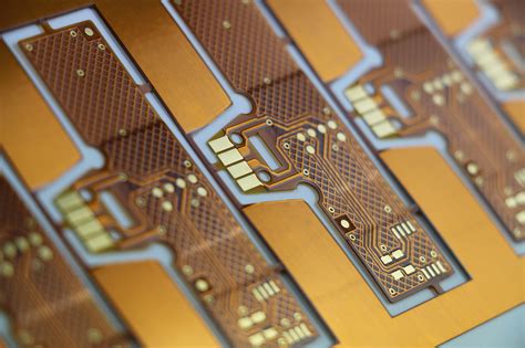
Flex PCB Materials
The choice of materials plays a crucial role in the performance and reliability of flex PCBs. Let’s explore the commonly used materials in flex PCB construction:
Substrate Materials
The substrate is the foundation of a flex PCB, providing the base for the conductive traces and components. The most common substrate materials used in flex PCBs are:
-
Polyimide (PI): Polyimide is the most widely used substrate material for flex PCBs due to its excellent thermal stability, chemical resistance, and mechanical strength. It can withstand high temperatures and has a low coefficient of thermal expansion (CTE).
-
Polyester (PET): Polyester is a cost-effective alternative to polyimide for less demanding applications. It has good flexibility and electrical properties but lower temperature resistance compared to polyimide.
-
Liquid Crystal Polymer (LCP): LCP is a high-performance substrate material known for its low moisture absorption, excellent electrical properties, and dimensional stability. It is suitable for high-frequency applications.
Conductive Materials
The conductive traces and pads on a flex PCB are typically made of copper. The copper foil is laminated onto the substrate material and then etched to create the desired circuit pattern. The thickness of the copper foil is measured in ounces per square foot (oz/ft²), with common thicknesses being 1/2 oz, 1 oz, and 2 oz.
Coverlay and Solder Mask
To protect the copper traces and provide insulation, a coverlay or solder mask is applied to the flex PCB. Coverlay is a flexible film that is laminated onto the PCB, while solder mask is a protective coating that is screen printed or photoimaged onto the PCB. Both serve to insulate the traces, prevent short circuits, and provide protection against environmental factors.

Flex PCB Design Considerations
Designing a flex PCB requires careful consideration of various factors to ensure optimal performance and manufacturability. Here are some key design considerations to keep in mind:
Bend Radius and Flexibility
One of the most critical aspects of flex PCB design is determining the appropriate bend radius and flexibility requirements. The bend radius refers to the minimum radius that the PCB can be bent without causing damage or affecting its performance. It is essential to consider the thickness of the substrate, copper, and any stiffeners used when calculating the bend radius.
The flexibility of the PCB is influenced by factors such as the substrate material, copper thickness, and the presence of stiffeners or adhesives. It is crucial to design the PCB with the intended application and flexing requirements in mind to ensure reliable operation.
Trace Width and Spacing
When designing the conductive traces on a flex PCB, it is important to consider the trace width and spacing. The trace width should be sufficient to carry the required current without excessive heating or voltage drop. The spacing between traces should be adequate to prevent short circuits and maintain signal integrity.
The following table provides general guidelines for trace width and spacing based on the copper thickness:
| Copper Thickness (oz) | Minimum Trace Width (mm) | Minimum Spacing (mm) |
|---|---|---|
| 1/2 | 0.15 | 0.15 |
| 1 | 0.20 | 0.20 |
| 2 | 0.30 | 0.30 |
Stiffeners and Adhesives
In some cases, it may be necessary to use stiffeners or adhesives to provide additional support or rigidity to certain areas of the flex PCB. Stiffeners are typically made of materials such as polyimide or FR-4 and are laminated to the PCB in specific regions to prevent excessive flexing or to maintain a desired shape.
Adhesives can be used to bond the flex PCB to rigid sections or to other components. It is important to select adhesives that are compatible with the substrate material and can withstand the expected environmental conditions.
Panelization and Routing
Panelization is the process of arranging multiple PCB designs on a single panel for efficient manufacturing. When panelizing flex PCBs, it is essential to consider the placement of the designs to minimize waste and ensure proper routing.
Routing refers to the process of cutting the individual PCBs from the panel. For flex PCBs, routing can be done using a variety of methods, including steel rule die cutting, laser cutting, or CNC routing. The choice of routing method depends on factors such as the complexity of the design, the required precision, and the volume of production.

Flex PCB Manufacturing Process
The manufacturing process for flex PCBs involves several steps that are similar to those used for rigid PCBs, with some additional considerations specific to flexible circuits. Let’s walk through the typical steps involved in flex PCB manufacturing:
-
Design and Artwork Creation: The first step is to create the PCB design using CAD software and generate the necessary artwork files for manufacturing. The artwork includes the copper trace patterns, solder mask, and silkscreen layers.
-
Material Selection and Preparation: The appropriate substrate material, copper foil, and other materials are selected based on the design requirements. The substrate material is cut to the required size, and the copper foil is laminated onto it using heat and pressure.
-
Imaging and Etching: The copper-clad substrate is then coated with a photoresist material and exposed to UV light through a photomask containing the circuit pattern. The exposed areas of the photoresist are developed and removed, leaving the desired copper traces. The unwanted copper is etched away using a chemical etching process.
-
Lamination and Drilling: If the design requires multiple layers, the etched layers are laminated together using heat and pressure. Any necessary holes or vias are drilled through the laminated board.
-
Coverlay and Solder Mask Application: The coverlay or solder mask is applied to the PCB to protect the copper traces and provide insulation. The coverlay is laminated onto the PCB, while the solder mask is screen printed or photoimaged.
-
Surface Finishing: To enhance solderability and protect the exposed copper, a surface finish is applied to the PCB. Common surface finishes for flex PCBs include ENIG (Electroless Nickel Immersion Gold), OSP (Organic Solderability Preservative), and immersion silver.
-
Cutting and Routing: The individual PCBs are cut from the panel using the chosen routing method, such as steel rule die cutting or laser cutting. Any necessary slots or cutouts are also created during this step.
-
Inspection and Testing: The manufactured flex PCBs undergo thorough inspection and testing to ensure they meet the required quality standards. Visual inspection, continuity testing, and functional testing are performed to verify the integrity of the PCBs.
Best Practices for Flex PCB Assembly
To ensure a successful flex PCB assembly, consider the following best practices:
-
Choose the Right Materials: Select the appropriate substrate material, copper thickness, and surface finish based on the application requirements, such as flexibility, temperature resistance, and signal integrity.
-
Follow Design Guidelines: Adhere to the recommended design guidelines for trace width, spacing, bend radius, and panelization to ensure manufacturability and reliable performance.
-
Use Appropriate Stiffeners and Adhesives: If required, use stiffeners and adhesives judiciously to provide support and rigidity where needed without compromising flexibility.
-
Consider Strain Relief: Incorporate strain relief features, such as curves or loops, in the PCB design to minimize stress on the copper traces during flexing.
-
Optimize Panelization: Arrange the PCB designs on the panel to maximize material utilization and minimize waste. Consider the routing method and any specific manufacturing constraints.
-
Collaborate with Experienced Manufacturers: Work with experienced flex PCB manufacturers who have the necessary expertise, equipment, and processes to produce high-quality flex PCBs.
-
Perform Thorough Testing: Conduct comprehensive testing, including mechanical and electrical tests, to ensure the flex PCBs meet the required specifications and can withstand the expected operating conditions.
Frequently Asked Questions (FAQ)
-
What is the difference between a flex PCB and a rigid PCB?
A flex PCB is made from flexible materials that allow it to bend and conform to different shapes, while a rigid PCB is made from a rigid substrate material and cannot be flexed. -
Can flex PCBs be used for high-current applications?
Yes, flex PCBs can be used for high-current applications by using thicker copper traces or multiple copper layers to handle the required current. -
How do I determine the appropriate bend radius for my flex PCB?
The bend radius depends on factors such as the substrate thickness, copper thickness, and the presence of stiffeners. Consult with your PCB manufacturer to determine the appropriate bend radius for your specific design. -
What are the common surface finishes used for flex PCBs?
Common surface finishes for flex PCBs include ENIG (Electroless Nickel Immersion Gold), OSP (Organic Solderability Preservative), and immersion silver. The choice of surface finish depends on the application requirements and the assembly process. -
Can flex PCBs be used in harsh environments?
Yes, flex PCBs can be designed to withstand harsh environments by selecting appropriate materials, using protective coatings, and incorporating robust design features. However, it is important to consider the specific environmental conditions and consult with your PCB manufacturer for guidance.
Conclusion
Flex PCBs offer numerous advantages, including flexibility, reduced weight and size, improved reliability, and enhanced signal integrity. By understanding the materials, design considerations, manufacturing processes, and best practices involved in flex PCB assembly, you can create a wonderful PCB that meets your application requirements.
When embarking on a flex PCB project, collaborate with experienced manufacturers who can provide guidance and support throughout the design and manufacturing process. By following the guidelines and best practices outlined in this article, you can ensure a successful outcome and achieve a high-quality flex PCB that performs reliably in your intended application.
No responses yet