Gerber Files (RS-274X)
Gerber files, also known as RS-274X files, are the industry standard for PCB design data exchange. These files contain the information needed to fabricate the PCB, including the copper layers, solder mask, silkscreen, and drill data. Gerber files are generated from the PCB design software and are used by the PCB manufacturer to create the physical board.
Importance of Gerber Files
- Accurate PCB Fabrication: Gerber files provide the precise data required for the PCB manufacturer to fabricate the board according to the designer’s specifications. This includes the exact dimensions, layer stackup, and component placement.
- Consistency: By using a standardized file format like Gerber, designers can ensure that their PCB design data is interpreted consistently by different manufacturers, reducing the risk of errors and misinterpretation.
- Efficiency: Gerber files streamline the PCB fabrication process by providing all the necessary information in a compact and easy-to-use format. This reduces the need for manual data entry and minimizes the chances of human error.
Common Gerber File Extensions
| Extension | Description |
|---|---|
| .GBR | Generic Gerber file extension |
| .GTL | Top copper layer |
| .GBL | Bottom copper layer |
| .GTO | Top overlay (silkscreen) |
| .GBO | Bottom overlay (silkscreen) |
| .GTS | Top solder mask |
| .GBS | Bottom solder mask |
| .GTP | Top paste mask |
| .GBP | Bottom paste mask |
Bill of Materials (BOM)
A Bill of Materials (BOM) is a comprehensive list of all the components required to assemble the PCBA. It includes information such as the component reference designator, manufacturer part number, description, quantity, and any additional notes. The BOM is essential for the PCBA manufacturer to procure the correct components and ensure that the assembly process runs smoothly.
Importance of BOM
- Component Procurement: The BOM provides the PCBA manufacturer with a clear list of the components needed for the assembly process. This allows them to source the components efficiently and avoid delays due to missing or incorrect parts.
- Cost Estimation: By having a detailed BOM, the PCBA manufacturer can accurately estimate the cost of the components and the overall assembly process. This helps in providing a precise quote to the customer and avoids any unexpected costs.
- Quality Control: The BOM serves as a reference for quality control during the assembly process. It helps ensure that the correct components are used and that the PCBA is assembled according to the designer’s specifications.
BOM Format
A typical BOM should include the following information:
| Column | Description |
|---|---|
| Item Number | A unique identifier for each component |
| Quantity | The number of each component required |
| Reference Designator | The reference designator assigned to the component in the schematic and PCB layout |
| Manufacturer Part Number | The unique part number assigned by the component manufacturer |
| Description | A brief description of the component, including its value, tolerance, and package type |
| Manufacturer | The name of the component manufacturer |
| Notes | Any additional information or special requirements for the component |
Pick and Place (PnP) File
A Pick and Place (PnP) file, also known as a centroid file or XY file, contains the coordinate information for the placement of components on the PCB. It is used by the automated pick and place machine to accurately position the components during the assembly process. The PnP file is generated from the PCB design software and includes details such as the component reference designator, X and Y coordinates, rotation, and side of the board.
Importance of PnP File
- Automated Assembly: The PnP file enables the use of automated pick and place machines, which significantly speeds up the assembly process and reduces the risk of human error. This is particularly important for high-volume production or PCBAs with a large number of components.
- Accurate Component Placement: By providing precise coordinate information, the PnP file ensures that components are placed accurately on the PCB. This is crucial for ensuring proper functionality and reliability of the PCBA.
- Efficiency: The PnP file streamlines the assembly process by eliminating the need for manual component placement. This reduces the time and labor required for assembly, resulting in faster turnaround times and lower production costs.
PnP File Format
A typical PnP file should include the following information:
| Column | Description |
|---|---|
| Ref | The reference designator assigned to the component in the schematic and PCB layout |
| Val | The value or description of the component |
| Package | The package type of the component |
| PosX | The X-coordinate of the component on the PCB |
| PosY | The Y-coordinate of the component on the PCB |
| Rot | The rotation of the component (in degrees) |
| Side | The side of the PCB where the component is placed (Top or Bottom) |

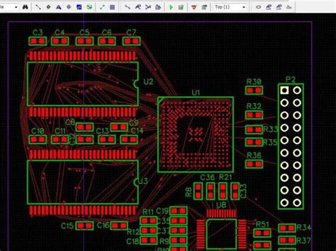
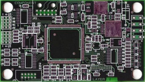
Assembly Drawing
An assembly drawing, also known as an assembly diagram or mechanical drawing, is a visual representation of the PCBA that provides clear instructions for the assembly process. It typically includes information such as the component placement, orientation, and any special assembly requirements. The assembly drawing helps ensure that the PCBA is assembled correctly and consistently, especially when manual assembly is involved.
Importance of Assembly Drawing
- Assembly Instructions: The assembly drawing serves as a visual guide for the assembly process, providing clear instructions on how the components should be placed and oriented on the PCB. This is particularly important for manual assembly or when dealing with complex PCBAs.
- Quality Control: By following the assembly drawing, the PCBA manufacturer can ensure that the assembly process is carried out consistently and accurately. This helps maintain the quality and reliability of the final product.
- Communication: The assembly drawing is an effective tool for communicating the designer’s intent to the PCBA manufacturer. It helps avoid misinterpretation and ensures that everyone involved in the assembly process is on the same page.
Assembly Drawing Elements
A typical assembly drawing should include the following elements:
- PCB outline: A clear representation of the PCB shape and dimensions.
- Component Placement: The location and orientation of each component on the PCB, including the reference designator and any specific placement requirements.
- Assembly Notes: Any special instructions or requirements for the assembly process, such as torque specifications, adhesive application, or special handling.
- Revision Information: The revision number and date of the assembly drawing, to ensure that the most up-to-date version is being used.
- Bill of Materials (BOM): A list of all the components required for the assembly, either included directly on the drawing or as a separate document.
Schematic Diagram
A schematic diagram is a graphical representation of the electronic circuit that shows the interconnections between components. It uses standardized symbols to represent the various components and their electrical connections. The schematic diagram is essential for understanding the circuit’s functionality and troubleshooting any issues that may arise during the assembly or testing process.
Importance of Schematic Diagram
- Circuit Understanding: The schematic diagram provides a clear and concise representation of the electronic circuit, allowing engineers and technicians to understand how the components are interconnected and how the circuit functions as a whole.
- Troubleshooting: In the event of any issues during the assembly or testing process, the schematic diagram is an invaluable tool for troubleshooting. It helps identify potential problems, such as incorrect connections or component failures, and guides the troubleshooting process.
- Design Verification: The schematic diagram is used to verify that the PCB design matches the intended electronic circuit. This helps catch any design errors early in the process, reducing the risk of costly mistakes during PCB fabrication and assembly.
Schematic Diagram Elements
A typical schematic diagram should include the following elements:
- Component Symbols: Standardized symbols representing the various electronic components, such as resistors, capacitors, transistors, and integrated circuits.
- Electrical Connections: Lines representing the electrical connections between components, showing how they are interconnected.
- Reference Designators: Unique identifiers assigned to each component, such as R1 for a resistor or U1 for an integrated circuit. These designators are used to cross-reference components between the schematic diagram, PCB layout, and BOM.
- Values and Ratings: The values and ratings of the components, such as resistance values for resistors or voltage ratings for capacitors.
- Notes and Labels: Any additional notes or labels that provide clarification or special instructions related to the circuit.
Frequently Asked Questions (FAQ)
-
What happens if I don’t provide all the necessary files for PCBA?
If you don’t provide all the necessary files, the PCBA manufacturer may not be able to proceed with the fabrication and assembly process. They will likely request the missing files, which can cause delays in the project timeline. In some cases, the manufacturer may be able to work with partial information, but this can increase the risk of errors and inconsistencies in the final product. -
Can I use different CAD software to generate the files for PCBA?
Yes, you can use different CAD software to generate the files for PCBA, as long as the software can export the files in the required formats. Most modern PCB design software packages can generate Gerber files, BOMs, and PnP files that are compatible with industry standards. However, it’s always a good idea to check with your PCBA manufacturer to ensure that the files you provide are in a format they can work with. -
What should I do if I need to make changes to the PCBA design after submitting the files?
If you need to make changes to the PCBA design after submitting the files, you should notify your PCBA manufacturer as soon as possible. Depending on the stage of the fabrication and assembly process, the changes may be able to be incorporated without significant delays or additional costs. However, if the changes are requested after the PCB fabrication has begun or components have been procured, there may be additional charges and longer lead times. -
How can I ensure that my files are error-free before submitting them to the PCBA manufacturer?
To ensure that your files are error-free, you should thoroughly review and double-check all the information before submitting them to the PCBA manufacturer. This includes verifying that the Gerber files match the intended PCB design, the BOM is complete and accurate, and the PnP file coordinates are correct. Many PCB design software packages include tools for design rule checks (DRC) and error checking, which can help identify potential issues before exporting the files. -
What are the benefits of providing a complete and accurate set of files for PCBA?
Providing a complete and accurate set of files for PCBA has several benefits: - Faster turnaround times, as the manufacturer has all the necessary information to proceed with the fabrication and assembly process without delays.
- Reduced risk of errors and inconsistencies in the final product, as the manufacturer can work with precise and reliable data.
- Improved communication and collaboration between the designer and the manufacturer, as all the required information is clearly presented and understood by both parties.
- Potential cost savings, as complete and accurate files can help avoid unnecessary revisions, delays, or scrap due to incorrect or missing information.
In conclusion, providing the essential files for PCBA, including Gerber files, BOM, PnP file, assembly drawing, and schematic diagram, is crucial for ensuring a smooth and efficient manufacturing process. These files provide the necessary information for PCB fabrication, component procurement, automated assembly, and quality control. By taking the time to generate complete and accurate files, designers can collaborate effectively with PCBA manufacturers, reducing the risk of errors, delays, and additional costs.
No responses yet