What are Fiducial PCBs?
Fiducial PCBs, also known as Fiducial Markers or fiducial points, are specialized printed circuit boards used for precise positioning and alignment during the assembly and manufacturing process of electronic devices. These unique PCBs serve as reference points that help machine vision systems accurately locate and orient components on the main PCB, ensuring proper placement and reducing the risk of assembly errors.
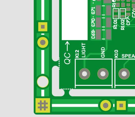
Fiducial PCBs typically feature a set of three or more distinct, high-contrast markers strategically placed on the board’s surface. These markers are usually circular or crosshair-shaped and are made from materials that are easily recognizable by the machine vision systems, such as copper, gold, or solder mask.
Key Characteristics of Fiducial PCBs
| Characteristic | Description |
|---|---|
| Shape | Circular or crosshair |
| Size | Typically 1-3mm in diameter |
| Material | Copper, gold, or solder mask |
| Quantity | Minimum of three markers per PCB |
| Placement | Strategic locations for optimal recognition |
The Importance of Fiducial PCBs in Electronics Manufacturing
Fiducial PCBs play a crucial role in the electronics manufacturing industry, particularly in the surface mount technology (SMT) process. As electronic devices become increasingly complex and miniaturized, the need for precise component placement grows exponentially. Even the slightest misalignment can lead to malfunctions, reduced performance, or complete device failure.
By incorporating fiducial PCBs into the manufacturing process, companies can achieve several key benefits:
-
Improved accuracy: Fiducial markers enable machine vision systems to accurately locate and orient components, reducing the risk of misalignment and ensuring consistent quality across production runs.
-
Increased efficiency: Automated assembly processes that utilize fiducial PCBs can operate at higher speeds and with fewer errors, resulting in improved overall production efficiency.
-
Cost reduction: By minimizing assembly errors and increasing production speed, fiducial PCBs help reduce manufacturing costs associated with rework, scrap, and downtime.
-
Enhanced reliability: Properly aligned components contribute to the overall reliability and longevity of the final product, reducing the likelihood of premature failure or performance issues.

Designing Fiducial PCBs
When designing fiducial PCBs, several key factors must be considered to ensure optimal performance and compatibility with the manufacturing process.
Marker Placement
The placement of fiducial markers on the PCB is critical for accurate recognition by the machine vision system. Typically, a minimum of three markers are required, with one located near each corner of the board. This configuration allows the vision system to triangulate the board’s position and orientation accurately.
In some cases, additional markers may be necessary, particularly for larger or more complex PCBs. When placing markers, designers must ensure that they are not obscured by components, solder paste, or other features on the board.
Marker Size and Shape
Fiducial markers are typically designed as circular or crosshair-shaped features, as these shapes are easily recognizable by machine vision systems. The size of the markers is also important, with most manufacturers recommending a diameter between 1mm and 3mm.
Smaller markers may be more challenging for the vision system to detect, while larger markers can consume valuable board space and potentially interfere with component placement. Designers must strike a balance between marker size and board layout to ensure optimal performance.
Material Selection
The material used for fiducial markers must provide sufficient contrast against the PCB substrate to ensure reliable detection by the machine vision system. Common materials include copper, gold, and solder mask.
Copper markers are often preferred due to their low cost and compatibility with standard PCB fabrication processes. Gold markers offer excellent contrast but are more expensive and may require additional processing steps. Solder mask markers, created by selectively removing the solder mask to expose the underlying copper, provide good contrast and are easily integrated into the PCB design.
Clearance and Solder Mask Openings
To ensure accurate detection by the machine vision system, fiducial markers must be surrounded by a clear area free of components, solder paste, or other features. This clearance area, typically 1-2mm in width, helps prevent obstruction and ensures a clean, high-contrast image for the vision system to process.
In addition to the clearance area, designers must also specify the appropriate solder mask openings for the fiducial markers. These openings, typically slightly larger than the marker itself, expose the underlying copper and provide the necessary contrast for reliable detection.

Integrating Fiducial PCBs into the Manufacturing Process
To fully realize the benefits of fiducial PCBs, manufacturers must properly integrate them into the overall production process. This involves several key steps:
-
Machine vision system setup: The machine vision system must be configured to recognize the specific size, shape, and material of the fiducial markers used on the PCB. This typically involves capturing reference images of the markers and defining the necessary detection parameters.
-
Alignment and calibration: Prior to production, the machine vision system must be aligned and calibrated using a known reference PCB with fiducial markers. This process ensures that the vision system can accurately locate and orient the PCB during the actual assembly process.
-
Pick-and-place programming: The pick-and-place machine, which is responsible for placing components on the PCB, must be programmed to use the fiducial markers as reference points. This involves defining the location of each marker relative to the board origin and specifying the required placement accuracy for each component.
-
Quality control and inspection: After the assembly process is complete, the machine vision system can be used to verify the accurate placement of components by comparing their actual positions to the expected locations based on the fiducial markers. This automated inspection process helps identify any assembly errors and ensures consistent quality across production runs.

Frequently Asked Questions (FAQ)
1. Can fiducial PCBs be used with both through-hole and surface mount components?
Yes, fiducial PCBs can be used in the assembly of both through-hole and surface mount components. However, they are most commonly used in surface mount technology (SMT) processes, where precise component placement is critical.
2. How does the number of fiducial markers affect the accuracy of the assembly process?
In general, using more fiducial markers can improve the accuracy of the assembly process, as it provides the machine vision system with additional reference points for locating and orienting the PCB. However, the optimal number of markers depends on factors such as the size and complexity of the PCB, the required placement accuracy, and the capabilities of the machine vision system.
3. Are there any specific design guidelines for fiducial markers?
Yes, there are several design guidelines to consider when creating fiducial markers:
– Use circular or crosshair-shaped markers for easy recognition by the machine vision system.
– Ensure markers are sized appropriately (typically 1-3mm in diameter) for reliable detection.
– Choose high-contrast materials such as copper, gold, or solder mask for the markers.
– Provide adequate clearance around the markers to prevent obstruction by components or solder paste.
– Specify the appropriate solder mask openings to expose the markers and enhance contrast.
4. Can fiducial PCBs be used in conjunction with other alignment methods?
Yes, fiducial PCBs can be used in combination with other alignment methods, such as edge detection or pin alignment, to further enhance the accuracy and reliability of the assembly process. In some cases, multiple alignment methods may be necessary to achieve the required level of precision.
5. Are there any limitations or drawbacks to using fiducial PCBs?
While fiducial PCBs offer significant benefits in terms of assembly accuracy and efficiency, there are a few potential limitations to consider:
– Fiducial markers consume board space that could otherwise be used for components or routing.
– The additional design and fabrication requirements for fiducial markers may slightly increase the overall cost of the PCB.
– Proper machine vision system setup, calibration, and programming are essential for realizing the full benefits of fiducial PCBs, which may require specialized expertise and equipment.
Despite these limitations, the advantages of using fiducial PCBs in the electronics manufacturing process often far outweigh the drawbacks, making them an essential tool for ensuring high-quality, reliable product assembly.
Conclusion
Fiducial PCBs are a crucial component in the modern electronics manufacturing process, enabling high-precision component placement and assembly. By providing machine vision systems with clear reference points, these specialized PCBs help ensure accurate alignment, reduce assembly errors, and improve overall production efficiency.
As electronic devices continue to become more complex and miniaturized, the importance of fiducial PCBs will only continue to grow. By understanding the design principles, integration requirements, and potential limitations of fiducial PCBs, manufacturers can optimize their assembly processes and deliver high-quality, reliable products to their customers.
No responses yet