What is PCB Fabrication?
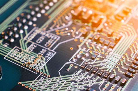
PCB fabrication is the process of manufacturing printed circuit boards (PCBs). PCBs are thin boards made of fiberglass, composite epoxy, or other laminate material that have conductive pathways etched or printed on them to create the electrical interconnections between electronic components. The PCB fabrication process involves several steps to take the PCB design and turn it into a physical board ready for components to be assembled onto it.
Key Steps in PCB Fabrication
The main steps involved in fabricating a printed circuit board are:
- Design: Creating the schematic design and PCB Layout using EDA (electronic design automation) software
- Printing: Printing the circuit pattern onto the copper layers of the PCB substrate material
- Etching: Chemically removing the unwanted copper to leave only the desired circuit traces
- Drilling: Drilling holes for vias and through-hole components
- Plating: Applying solder mask and silkscreen markings and plating exposed copper areas
- Finishing: Performing final inspection and electrical testing of the PCB
Types of PCBs
There are three main types of printed circuit boards:
Single Layer PCBs
Single layer PCBs have conductive copper traces printed on one side of the board only. The other side is left as bare substrate material. Single layer boards are the simplest and cheapest PCBs, but they are limited in the complexity of circuits that can be routed on them.
Double Layer PCBs
Double layer PCBs have copper traces on both sides of the board. The two copper layers are connected with vias. Double-sided boards allow for more complex circuits and a higher component density than single layer boards.
Multi-Layer PCBs
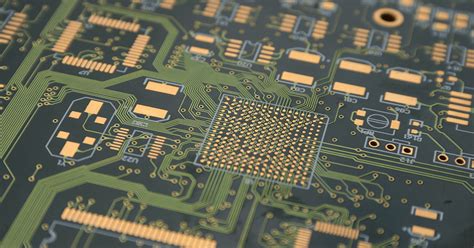
Multi-layer PCBs have three or more copper layers laminated together with insulating material in between each layer. The different layers are connected with vias. Having additional layers allows very complex and high density circuit designs. Most modern electronics use multi-layer PCBs.
| PCB Type | Layers | Cost | Density | Applications |
|---|---|---|---|---|
| Single Layer | 1 | Low | Low | Simple circuits |
| Double Layer | 2 | Medium | Medium | Common circuits |
| Multi-Layer | 3+ | High | High | Complex circuits |
PCB Materials
The base material used for the PCB substrate is typically FR-4 fiberglass. FR-4 is a composite material composed of woven fiberglass cloth with an epoxy resin binder. It provides good mechanical strength, electrical insulation, and temperature resistance.
Other PCB Substrate Materials include:
* Aluminum: used for metal core PCBs for better heat dissipation
* Polyimide: a flexible polymer used for flexible PCBs
* Ceramic: used for high frequency PCBs
* Teflon: used for high frequency PCBs
The copper foil used for the circuit layers is electrodeposited or rolled copper that is laminated to the substrate. The standard copper thickness for outer layers is 1 oz (35 um) or 2 oz (70 um). Inner layers typically use 0.5 oz (17.5 um) copper.

PCB Fabrication Process
Design
The first step in PCB fabrication is the design process. The circuit schematic is first created, which defines the electrical connections between components. Then the PCB layout is created from the schematic. The PCB layout determines the physical location of components and routing of traces on the board.
Printing
Once the PCB layout is complete, the circuit pattern is printed onto the copper layers. This is typically done using photoresist and a photomask. The photomask has a negative image of the circuit pattern. Photoresist is applied to the PCB and then exposed to light through the photomask. The areas of photoresist exposed to light harden and the rest can be washed away.
Etching
After the photoresist is developed, the unwanted copper is removed by etching. The hardened photoresist protects the desired copper circuit traces. Chemical etching is the most common method, typically using ammonium persulfate or ferric chloride. The etchant dissolves away the exposed copper, leaving only the circuit pattern under the photoresist.
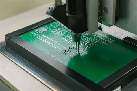
Drilling
Holes are drilled in the PCB for through-hole component leads and vias. Smaller vias may be laser drilled. The holes are drilled using a computer-controlled drill based on the drill file generated from the PCB design software.
Plating
After drilling, the holes are plated with copper to electrically connect the different layers. The outer layers of the PCB are also plated with copper to protect the traces.
A solder mask layer is applied to the PCB, leaving only the exposed pads and holes bare. The solder mask is usually green but can be other colors. It protects the copper traces and prevents solder bridges.
A silkscreen layer is applied to print component labels and identifiers on the PCB. The silkscreen is typically white but can be yellow or black.
Finishing
After plating, a surface finish is applied to the exposed copper to prevent oxidation and enhance solderability. The most common surface finishes are:
- HASL (Hot Air Solder Leveling): solder is applied to the copper and then leveled by hot air
- ENIG (Electroless Nickel Immersion Gold): a thin layer of gold over a nickel barrier is plated onto the copper
- OSP (Organic Solderability Preservatives): an organic compound is applied to the copper to prevent oxidation
- Immersion Silver: a thin layer of silver is chemically deposited onto the copper
| Finish | Cost | Shelf Life | Solderability | RoHS |
|---|---|---|---|---|
| HASL | Low | 12 months | Good | Varies |
| ENIG | High | 12 months+ | Excellent | Yes |
| OSP | Low | 6 months | OK | Yes |
| Immersion Silver | Medium | 12 months | Good | Yes |
The finished PCBs go through a final visual inspection and electrical testing to check for defects. The PCBs are then packaged and shipped to the customer for assembly.
PCB Design Considerations
There are several things that need to be considered when designing a PCB for manufacturing:
Minimum Trace Width and Spacing
The minimum trace width and spacing depends on the PCB manufacturer’s capabilities. Typically, smaller traces and spaces cost more due to the tighter tolerances required. Most PCB fabs can do 5 mil (0.127 mm) traces and spaces, and 4 mil (0.102 mm) is becoming more common.
Minimum Drill Size
The minimum hole size that can be mechanically drilled is typically 8 mil (0.203 mm) in diameter. Smaller holes down to 4 mil (0.102 mm) can be laser drilled but cost more. Vias typically start at 10 mil (0.254 mm).
Minimum Annular Ring
The annular ring is the copper pad around a drilled hole. The minimum annular ring depends on the hole size and layer count. For a typical 8 mil hole, the minimum annular ring is about 4 mil.
Solder Mask and Silkscreen
The minimum solder mask web is typically 4 mil (0.102 mm). The minimum silkscreen line width is usually 5 mil (0.127 mm). Text should be at least 40 mil (1.016 mm) in height. Smaller sizes may be possible but cost more.
Panelization
PCBs are often panelized into an array to make assembly more efficient. Panelization also makes better use of the material resulting in a lower cost per PCB. However, the panel size is limited by the PCB manufacturer’s equipment. Common panel sizes are 18″ x 24″ (457 mm x 610 mm) in the US and 330 mm x 250 mm in Europe. The rails between boards are typically 5 mm to 10 mm wide.
Choosing a PCB Manufacturer
There are hundreds of PCB manufacturers around the world, so it can be difficult to know which one to choose. Here are some things to consider when selecting a PCB fab:
Capabilities
Make sure the PCB manufacturer can handle your technical requirements such as number of layers, material, minimum trace and space, hole sizes, surface finish, etc. Not all PCB fabs have the same capabilities.
Quality
The PCB fabricator should have a good quality management system in place and be ISO 9001 certified. Look for a manufacturer that does electrical testing and has a low defect rate.
Cost
Of course, cost is always a factor. Get quotes from several PCB manufacturers and compare prices. But don’t just go with the lowest price – make sure to also consider quality and capabilities.
Lead Time
The turnaround time for PCB fabrication can vary from a few days to several weeks depending on the complexity and quantity. Make sure the manufacturer can meet your schedule requirements.
Communication
Good communication is important in case there are any issues with the design or manufacturing process. Choose a PCB manufacturer that is responsive and easy to work with.
FAQ
How much does PCB fabrication cost?
The cost of PCB fabrication depends on several factors such as number of layers, size, quantity, materials, surface finish, and turnaround time. In general, a simple 2-layer PCB will cost around $1-$5 per board in quantities of 100. More complex boards with 4 or more layers will cost $10-$50 per board.
What is the typical turnaround time for PCB fabrication?
The standard lead time for PCB Prototyping is about 1-2 weeks. For production quantities, lead times can be 3-4 weeks or more. Expedited turn times of 1-5 days are available from some manufacturers but cost more.
What is the minimum quantity for PCB fabrication?
Most PCB manufacturers have a minimum order quantity (MOQ) of 5-10 boards for prototyping. For production, the MOQ is typically 100-500 boards. Some manufacturers specialize in low volume production and can do smaller quantities.
What file formats are needed for PCB fabrication?
The most common file format for PCB fabrication is Gerber RS-274X. Gerber files are ASCII vector format files that describe each layer of the PCB. The drill file that specifies the location and size of holes is typically in Excellon format. A pick and place file that has the coordinates of each component is usually provided in CSV or ASCII format.
What are the most common problems with PCB fabrication?
Some of the most common issues with PCB manufacturing include:
- Incorrect or missing Gerber files
- Traces or spaces that are too small for the manufacturer’s capabilities
- Insufficient annular ring around holes
- Acid traps and starved thermals in the PCB layout
- Incorrectly sized or placed vias and component footprints
- Silkscreen text that is too small to be readable
- Not following the manufacturer’s design guidelines
Most of these issues can be caught and corrected in the design phase by doing a design for manufacturability (DFM) check. Many PCB manufacturers will do a free DFM check before starting fabrication.
Conclusion
PCB fabrication is a complex process with many steps and variables. It’s important to carefully design your PCB and choose a reputable manufacturer to ensure you get high-quality boards that meet your requirements. By understanding the basics of the PCB fabrication process and design guidelines, you can avoid common pitfalls and get your PCB project off to a good start.
No responses yet