Introduction to PCB stackup
PCB stackup refers to the arrangement of layers in a printed circuit board (PCB). It is a crucial aspect of PCB design, as it determines the board’s electrical properties, signal integrity, and manufacturability. A well-designed PCB stackup ensures that the board functions as intended and meets the required specifications.
Key Components of a PCB Stackup
A typical PCB stackup consists of the following components:
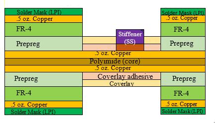
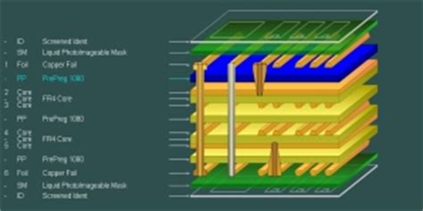
- Core layers: These are the main structural layers of the PCB, usually made of FR-4 material.
- Copper layers: These are the conductive layers that carry electrical signals and power. They are typically made of copper foil laminated onto the core layers.
- Prepreg layers: These are thin layers of pre-impregnated fiberglass used to bond the core layers together.
- Solder mask: This is a protective layer applied to the outer surfaces of the PCB to prevent short circuits and improve solderability.
- Silkscreen: This is a layer of text and symbols printed on the PCB for identification and assembly purposes.
Factors to Consider in PCB Stackup Design
When designing a PCB stackup, several factors must be considered to ensure optimal performance and manufacturability.
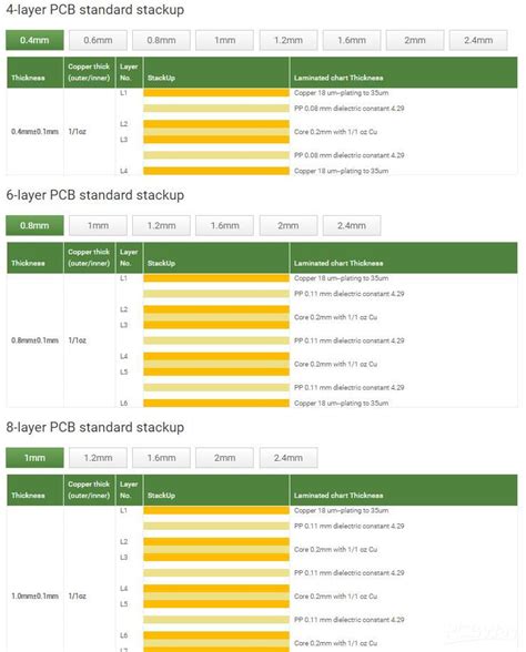
1. Number of Layers
The number of layers in a PCB stackup depends on the complexity of the circuit and the required functionality. A simple design may only require two layers (top and bottom), while more complex designs may need four, six, or even more layers.
| Number of Layers | Typical Applications |
|---|---|
| 2 | Simple circuits, low-speed digital designs |
| 4 | Most common, suitable for moderate complexity |
| 6 or more | High-speed designs, dense layouts, complex functionality |
2. Layer Thickness
The thickness of each layer in the PCB stackup affects the board’s mechanical strength, impedance control, and thermal management. Typical layer thicknesses are:
| Layer Type | Thickness (mm) |
|---|---|
| Core | 0.2 – 1.6 |
| Prepreg | 0.1 – 0.4 |
| Copper | 0.018 – 0.07 |
3. Material Selection
The choice of materials for the core, prepreg, and copper layers affects the PCB’s electrical and mechanical properties. FR-4 is the most common core material, while high-frequency laminates like Rogers or Isola may be used for high-speed designs.
4. Impedance Control
Controlling the impedance of the PCB traces is essential for maintaining signal integrity, especially in high-speed designs. This is achieved by carefully selecting the layer thicknesses, trace widths, and dielectric constants of the materials.
5. Signal Integrity
Ensuring signal integrity involves minimizing crosstalk, reflections, and other signal distortions. This can be achieved through proper layer arrangement, ground plane placement, and the use of techniques like differential routing and shielding.
Best Practices for PCB Stackup Design
To create a successful PCB stackup, follow these best practices:
- Start with a well-defined schematic and component placement.
- Choose the appropriate number of layers based on the circuit complexity and required functionality.
- Select materials that meet the electrical, mechanical, and thermal requirements of the design.
- Use a symmetrical stackup to minimize warpage and stress.
- Place ground and power planes adjacent to signal layers to provide shielding and reduce crosstalk.
- Use appropriate trace widths and spacing to control impedance and minimize signal distortions.
- Follow the manufacturer’s guidelines for minimum feature sizes and clearances.
- Verify the stackup design with a PCB fabricator to ensure manufacturability and cost-effectiveness.

Advanced PCB Stackup Techniques
For more complex designs, additional techniques can be employed to optimize the PCB stackup:
1. High-Density Interconnect (HDI)
HDI involves using microvias and buried or blind vias to create more compact layouts and improve signal routing. This technique is particularly useful for high-speed designs and designs with limited board space.
2. Rigid-Flex PCBs
Rigid-flex PCBs combine rigid and flexible layers to create a board that can bend or fold. This technique is useful for applications that require compact packaging or dynamic flexing.
3. Embedded Components
Embedding components like capacitors or resistors within the PCB stackup can save board space and improve electrical performance. This technique requires careful planning and coordination with the PCB fabricator.
Conclusion
Designing a successful PCB stackup requires careful consideration of various factors, including the number of layers, material selection, impedance control, and signal integrity. By following best practices and employing advanced techniques when necessary, designers can create PCB stackups that meet the required specifications and ensure optimal performance.
Frequently Asked Questions (FAQ)
1. What is the most common number of layers in a PCB stackup?
Four-layer PCBs are the most common, as they provide a good balance between complexity and cost for most applications.
2. What is the purpose of ground planes in a PCB stackup?
Ground planes provide a low-impedance return path for signals, shield against electromagnetic interference (EMI), and help to control impedance.
3. What is the difference between a core layer and a prepreg layer?
Core layers are the main structural layers of the PCB, while prepreg layers are thin, pre-impregnated fiberglass layers used to bond the core layers together.
4. How does the choice of materials affect the PCB stackup design?
The choice of materials affects the PCB’s electrical properties (e.g., dielectric constant, loss tangent), mechanical strength, and thermal management. Different materials may be selected based on the specific requirements of the design.
5. What are the benefits of using HDI techniques in PCB stackup design?
HDI techniques, such as microvias and buried or blind vias, allow for more compact layouts, improved signal routing, and better electrical performance. They are particularly useful for high-speed designs and designs with limited board space.
No responses yet