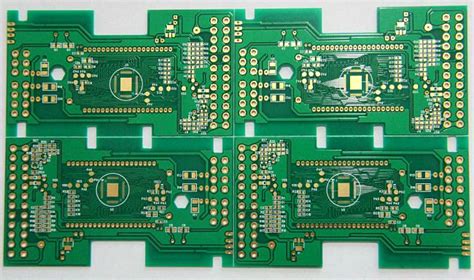
What is PCB Etching?
PCB etching is the process of removing unwanted copper from a PCB substrate to create the desired circuit pattern. The copper layer is initially laminated onto the substrate, and then a resist layer is applied on top of the copper in the shape of the circuit design. The etching process removes the exposed copper, leaving behind only the copper traces protected by the resist.
Wet Etching
Wet etching is the most common method for PCB etching, especially for small-scale productions and hobbyist projects. This process involves submerging the PCB in a chemical solution that dissolves the exposed copper.
Wet Etching Process
- PCB preparation: The PCB is cleaned and a photoresist layer is applied to the copper surface.
- Exposing the resist: The photoresist is exposed to UV light through a photomask, hardening the areas that will form the copper traces.
- Developing the resist: The unexposed photoresist is removed using a developer solution, leaving the hardened resist in the shape of the circuit pattern.
- Etching the copper: The PCB is submerged in an etching solution, typically ferric chloride or ammonium persulfate, which dissolves the exposed copper.
- Stripping the resist: After etching, the remaining photoresist is removed using a stripping solution, revealing the final copper traces.
Advantages of Wet Etching
- Low cost and simple setup
- Suitable for small-scale productions and hobbyist projects
- Relatively fast process
- Can handle complex designs with fine details
Disadvantages of Wet Etching
- Limited control over the etching process
- Potential for over-etching or undercutting of copper traces
- Requires handling and disposal of hazardous chemicals
- Slower than dry etching for high-volume production

Dry Etching
Dry etching, also known as plasma etching, is a more advanced method that uses a plasma (ionized gas) to remove the unwanted copper. This process is more commonly used in industrial settings and for high-volume PCB production.
Dry Etching Process
- PCB preparation: Similar to wet etching, the PCB is cleaned and a photoresist layer is applied.
- Exposing and developing the resist: The photoresist is exposed and developed as in the wet etching process.
- Plasma etching: The PCB is placed in a vacuum chamber, and a plasma is generated using a high-frequency electromagnetic field. The plasma contains reactive ions that bombard the exposed copper, etching it away.
- Stripping the resist: The remaining photoresist is removed, revealing the final copper traces.
Advantages of Dry Etching
- High precision and control over the etching process
- Minimal undercutting of copper traces
- Faster than wet etching for high-volume production
- No need for hazardous chemicals
- Suitable for very fine pitch designs
Disadvantages of Dry Etching
- Higher equipment and operating costs
- More complex setup and maintenance
- Requires skilled operators
- May not be cost-effective for small-scale productions

Comparison Table
| Factor | Wet Etching | Dry Etching |
|---|---|---|
| Cost | Low | High |
| Setup Complexity | Simple | Complex |
| Etching Speed | Moderate | Fast |
| Precision | Moderate | High |
| Undercutting | Potential Issue | Minimal |
| Chemical Handling | Required | Not Required |
| Suitable Scales | Small to Medium | High Volume |

FAQ
1. Can I use wet etching for high-volume PCB production?
While wet etching can be used for high-volume production, it is generally slower and less efficient than dry etching. Dry etching is better suited for large-scale manufacturing due to its higher precision and faster etching speed.
2. Is dry etching suitable for hobbyist projects?
Dry etching equipment is typically more expensive and complex than wet etching setups, making it less practical for hobbyist projects. Wet etching is generally more accessible and cost-effective for small-scale projects and prototyping.
3. What safety precautions should I take when using wet etching chemicals?
When handling wet etching chemicals, always wear appropriate personal protective equipment (PPE), such as gloves, safety glasses, and a lab coat. Work in a well-ventilated area and avoid skin contact or inhalation of fumes. Properly dispose of used etching solutions according to local regulations.
4. Can dry etching handle complex PCB designs with fine details?
Yes, dry etching is particularly well-suited for complex PCB designs with fine details and very fine pitch traces. The high precision and minimal undercutting of dry etching allow for the creation of intricate circuit patterns.
5. How do I choose between wet and dry etching for my PCB project?
The choice between wet and dry etching depends on several factors, such as the scale of production, required precision, budget, and available resources. For small-scale projects and prototyping, wet etching is often the most practical choice. For high-volume production and designs requiring high precision, dry etching is generally the preferred method.
Conclusion
Both wet and dry etching have their place in PCB manufacturing, each with its own advantages and disadvantages. Wet etching is a simple and cost-effective solution for small-scale projects and hobbyists, while dry etching offers high precision and efficiency for industrial-scale production. When deciding between the two methods, consider your project requirements, budget, and available resources to determine the best approach for your specific needs.
By understanding the differences between wet and dry etching, you can make an informed decision and optimize your PCB manufacturing process. Whether you’re a hobbyist working on a small project or an engineer overseeing high-volume production, selecting the appropriate etching method is crucial for achieving high-quality, reliable PCBs.
No responses yet